

A kind of semiconductor device with narrow line width and preparation method thereof
A semiconductor and narrow line width technology, applied in the field of narrow line width semiconductor devices and their preparation, can solve the problems of simple structure, inability to take into account the line width and high integration degree at the same time with light
- Summary
- Abstract
- Description
- Claims
- Application Information
AI Technical Summary
Problems solved by technology
Method used
Image

Examples
Embodiment Construction
[0024] At present, the methods to realize semiconductor devices with low spectral linewidth mainly include external cavity modulation feedback, device integration grating and other methods. For the external cavity feedback modulation method, the integration degree of the device is reduced due to the external cavity part; for the method of device integrated grating, the structure of the grating is complex, so the grating preparation process is more complicated, and it is difficult to improve the yield and efficiency of production.
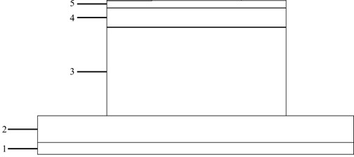
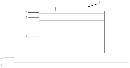
[0025] In recent years, topological photonics is a rapidly emerging research field, which uses geometric and topological ideas to design and control the behavior of light. This patent uses topological defect states and Fano resonance to design a semiconductor device with a narrow line width. This design can be realized only by growing layers with high and low refractive indices, while taking into account narrow line width, simple structure, and high ...
PUM
| Property | Measurement | Unit |
|---|---|---|
| transmittivity | aaaaa | aaaaa |
Abstract
Description
Claims
Application Information