Supercharge Your Innovation With Domain-Expert AI Agents!

Single-layer MoS2-Si-based tunneling diode and preparation method thereof

A tunneling diode, mos2-si technology, applied in the field of single-layer MoS2-Si-based tunneling diodes and its preparation, can solve subthreshold slew rate and off-state characteristics deterioration, trap-assisted tunneling, poor device performance, etc. problems, achieve the effect of reducing interface defect density, high-performance heterogeneous integrated system, and alleviating thermal expansion coefficient mismatch

Active Publication Date: 2021-11-12
XIDIAN UNIV
View PDF10 Cites 0 Cited by
  • Summary
  • Abstract
  • Description
  • Claims
  • Application Information

AI Technical Summary

Problems solved by technology

However, in terms of material selection, the traditional Si-based TFET has low tunneling efficiency due to its indirect bandgap and large forbidden band width. Deterioration of threshold slew rate and off-state characteristics
In addition, the heterojunction energy band structure that forms the type II energy band structure is the most ideal tunneling junction, but the heterogeneous tunneling junction formed by the bulk material in the traditional sense has serious lattice mismatch and trap-assisted tunneling. A series of problems, which in turn lead to poor device performance

Method used


Image

  • Single-layer MoS2-Si-based tunneling diode and preparation method thereof
  • Single-layer MoS2-Si-based tunneling diode and preparation method thereof
  • Single-layer MoS2-Si-based tunneling diode and preparation method thereof

Examples


Embodiment Construction

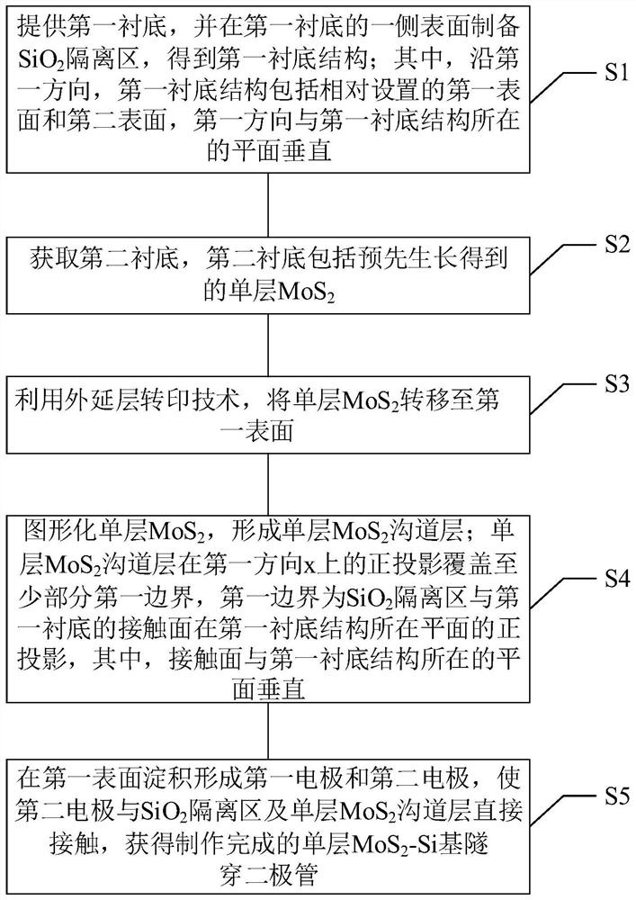
[0043] The present invention will be described in further detail below in conjunction with specific examples, but the embodiments of the present invention are not limited thereto.

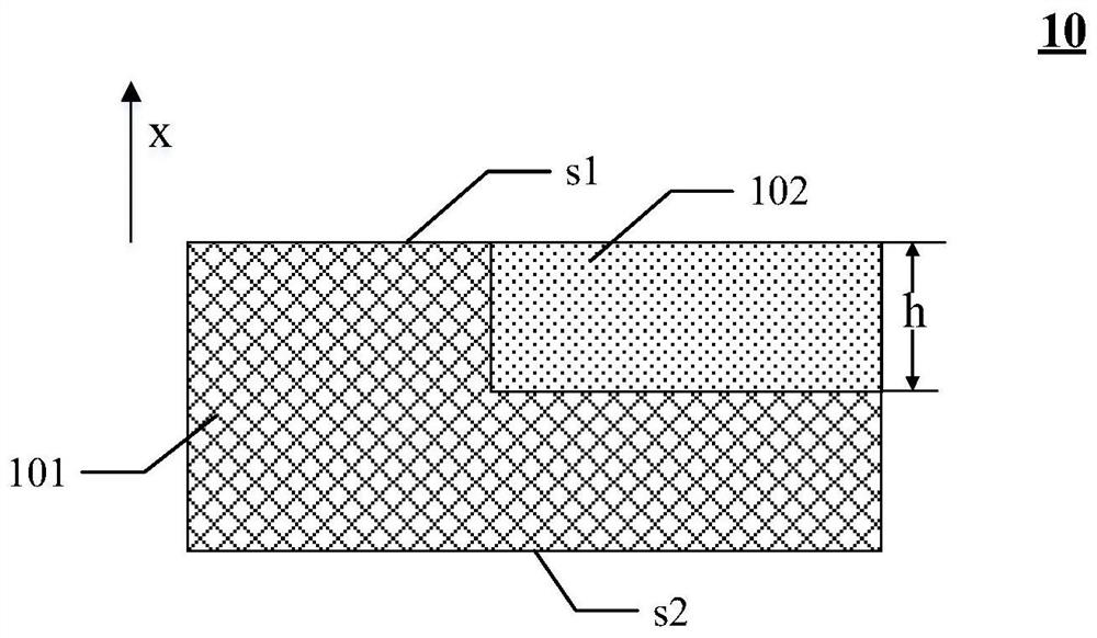
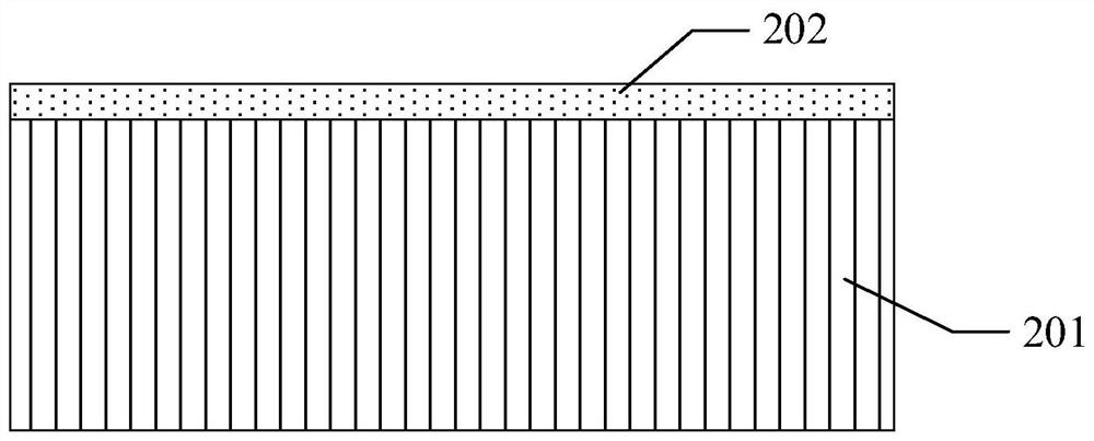
[0044] figure 1 It is the single-layer MoS provided by the embodiment of the present invention 2 - a schematic flow chart of the preparation method of Si-based tunneling diodes, Figure 2-6 It is the preparation of monolayer MoS provided by the embodiment of the present invention 2 -Schematic diagram of the process for Si-based tunneling diodes, Figure 7 It is the single-layer MoS provided by the embodiment of the present invention 2 -Schematic diagram of the structure of a Si-based tunneling diode. See Figure 1-7 , the present invention provides a single-layer MoS 2 -The preparation method of Si-based tunneling diode, comprising:

[0045] S1, providing a first substrate 101, and preparing SiO on one side surface of the first substrate 101 2 The isolation region 102 is used to obtain the ...


PUM

PropertyMeasurementUnit
thicknessaaaaaaaaaa
thicknessaaaaaaaaaa
thicknessaaaaaaaaaa

Abstract

The invention discloses a single-layer MoS2-Si-based tunneling diode and a preparation method thereof, and relates to the technical field of semiconductors, and the method comprises the steps: providing a first substrate, and preparing a SiO2 isolation region on the surface of one side of the first substrate to obtain a first substrate structure; obtaining a second substrate, wherein the second substrate comprises a single-layer MoS2 obtained through pre-growth; transferring the single-layer MoS2 to the first surface by using an epitaxial layer transfer printing technology; patterning the single-layer MoS2 to form a single-layer MoS2 channel layer; and depositing on the first surface to form a first electrode and a second electrode, enabling the second electrode to be in direct contact with the SiO2 isolation region and the single-layer MoS2 channel layer, and obtaining the manufactured single-layer MoS2-Si-based tunneling diode. According to the single-layer MoS2-Si-based tunneling diode and the preparation method thereof provided by the invention, the defect density of an interface can be reduced, trap-assisted tunneling is further inhibited, and the sub-threshold swing of a device is improved from a process angle.

Description

technical field [0001] The invention belongs to the field of semiconductor technology, in particular to a single-layer MoS 2 -Si-based tunneling diode and its preparation method. Background technique [0002] As the MOSFET (Metal-Oxide-Semiconductor Field-Effect Transistor, Metal-Oxide Semiconductor Field-Effect Transistor) device feature size gradually reaches deep submicron, the short channel effect appears, resulting in an increase in leakage current, which in turn reduces the power consumption of the device. Increased and reduced reliability, so ultra-steep devices need to be pursued. However, due to the Boltzmann smearing effect, the subthreshold swing of MOSFET cannot break through the limit of 60mV / dec at room temperature. This is determined by the conduction mechanism of MOSFET using hot electron transport. Therefore, ultra-steep devices with new mechanisms are sought without delay. [0003] In related technologies, a new device TFET (Tunneling Field-Effect Transi...

Claims


Application Information

Patent Timeline
Patent Type & Authority Applications(China)
IPC IPC(8): H01L29/88H01L21/329H01L29/267
CPCH01L29/88H01L29/66151H01L29/267Y02P70/50
Inventor 吕红亮贾紫骥孙佳乐吕智军张玉明张义门
Owner XIDIAN UNIV
Features
  • R&D
  • Intellectual Property
  • Life Sciences
  • Materials
  • Tech Scout
  • Unparalleled Data Quality
  • Higher Quality Content
  • 60% Fewer Hallucinations
Learn More