Supercharge Your Innovation With Domain-Expert AI Agents!

Formation method of semiconductor structure

A semiconductor and gate structure technology, applied in the field of semiconductor structure formation, can solve problems such as poor semiconductor structure performance, and achieve the effects of reducing influence, good performance, and reducing leakage current

Pending Publication Date: 2021-11-16
SEMICON MFG INT (SHANGHAI) CORP +1
View PDF0 Cites 0 Cited by
  • Summary
  • Abstract
  • Description
  • Claims
  • Application Information

AI Technical Summary

Problems solved by technology

[0004] However, when the source-drain doped region and the gate structure are electrically connected to the peripheral circuit through a common plug, the performance of the existing semiconductor structure is poor.

Method used


Image

  • Formation method of semiconductor structure
  • Formation method of semiconductor structure
  • Formation method of semiconductor structure

Examples


Embodiment Construction

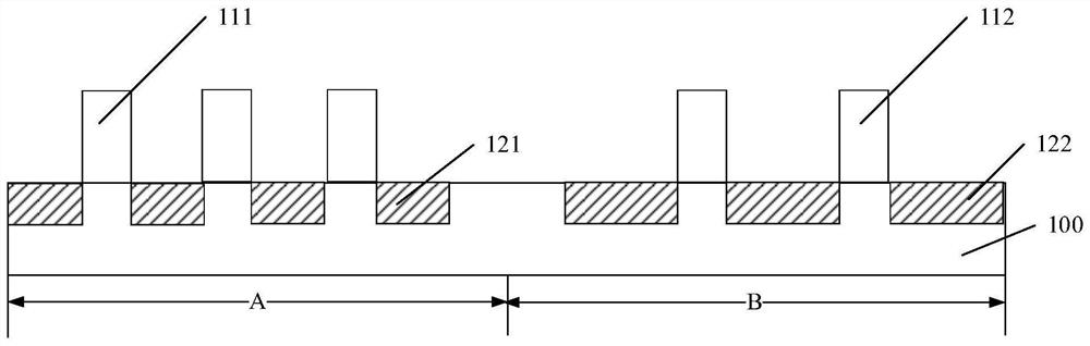
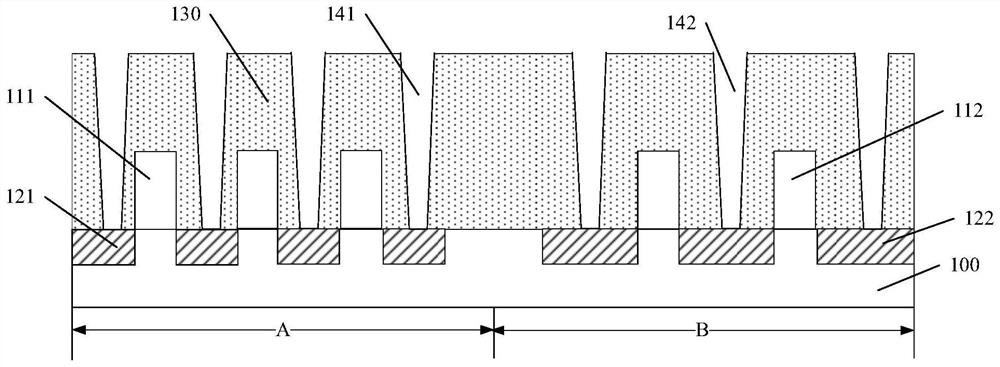
[0033] First, the reasons for the poor performance of existing semiconductor structures are described in detail in conjunction with the accompanying drawings, Figure 1 to Figure 4 It is a structural schematic diagram of each step of an existing method for forming a semiconductor structure.

[0034] Please refer to figure 1, providing a substrate 100, the substrate 100 includes a dense region A and a sparse region B, the dense region A has a plurality of first gate structures 111, and the substrate 100 on both sides of the first gate structure 111 has a first gate structure 111 respectively. A source-drain doped region 121 , the sparse region B has a plurality of second gate structures 112 , and the substrate 100 on both sides of the second gate structure 112 has second source-drain doped regions 122 respectively.

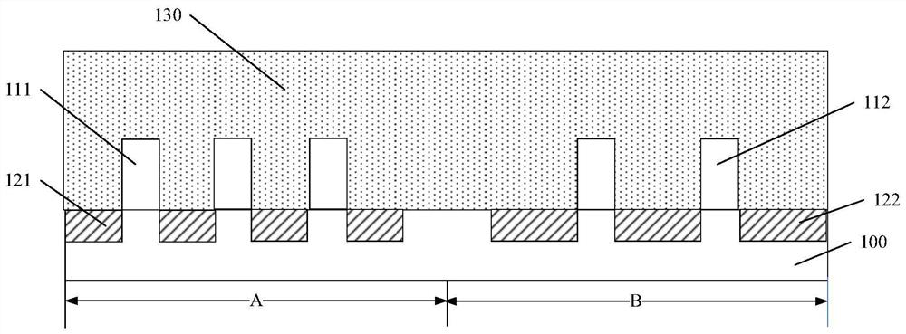
[0035] Please refer to figure 2 , form a dielectric layer 130 on the substrate 100, and the dielectric layer 130 is located in the first gate structure 111 and ...


PUM


Abstract

The invention discloses a formation method of a semiconductor structure, which comprises the steps of forming a plurality of first openings in a dielectric layer, wherein the bottom of each first opening exposes the top surface of a first source-drain doped region; forming a plurality of second openings in the dielectric layer, wherein the bottom of each second opening exposes part of the surface of the top of one first gate structure; and forming a plurality of third openings in the dielectric layer, wherein the bottom of each third opening is higher than the top surface of the first gate layer, and the third openings are communicated with the first openings and the second openings respectively. According to the method, mutual influence between different manufacturing processes can be reduced, so that the performance of the formed semiconductor structure is relatively good.

Description

technical field [0001] The invention relates to the technical field of semiconductor manufacturing, in particular to a method for forming a semiconductor structure. Background technique [0002] With the rapid development of semiconductor manufacturing technology, semiconductor devices are developing towards higher element density and higher integration. Transistors, as the most basic semiconductor devices, are being widely used at present. The control ability of traditional planar devices on channel current is weakened, resulting in short channel effect and leakage current, which ultimately affects the electrical performance of semiconductor devices. [0003] In order to overcome the short channel effect of the transistor and suppress the leakage current, the prior art proposes a fin field effect transistor (Fin FET), which is a common multi-gate device, and the structure of the fin field effect transistor includes : the fin and the isolation layer located on the surface o...

Claims


Application Information

Patent Timeline
Patent Type & Authority Applications(China)
IPC IPC(8): H01L21/336H01L21/8234H01L29/06
CPCH01L29/0638H01L29/66795H01L29/66545H01L21/823431
Inventor 赵炳贵
Owner SEMICON MFG INT (SHANGHAI) CORP
Features
  • R&D
  • Intellectual Property
  • Life Sciences
  • Materials
  • Tech Scout
  • Unparalleled Data Quality
  • Higher Quality Content
  • 60% Fewer Hallucinations
Learn More