Flip semiconductor light-emitting element, semiconductor light-emitting device and display device

A technology for light-emitting components and semiconductors, applied in semiconductor devices, electric solid-state devices, electrical components, etc., can solve problems such as poor die bonding, electrode pad breakage, affecting device reliability, etc., and achieve good morphology and enhanced adhesion. , the effect of enhancing stability and reliability

Active Publication Date: 2021-11-16
XIAMEN SANAN OPTOELECTRONICS CO LTD
View PDF6 Cites 1 Cited by
  • Summary
  • Abstract
  • Description
  • Claims
  • Application Information

AI Technical Summary

Problems solved by technology

When the electrode pad is formed, the electrode pad will also have a correspondingly uneven surface, which makes its coverage poor and there is a risk of fracture
In addition, in the subsequent die bonding process, it will also cause poor die bonding, and there will also be hidden dangers of electrode pad breakage, which will affect the reliability of the device.

Method used


Image

  • Flip semiconductor light-emitting element, semiconductor light-emitting device and display device
  • Flip semiconductor light-emitting element, semiconductor light-emitting device and display device
  • Flip semiconductor light-emitting element, semiconductor light-emitting device and display device

Examples


Embodiment 1

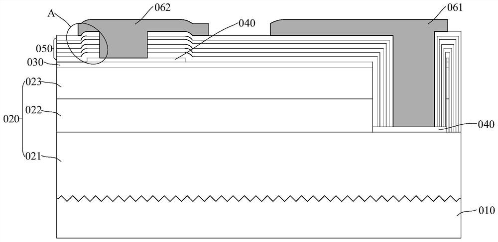
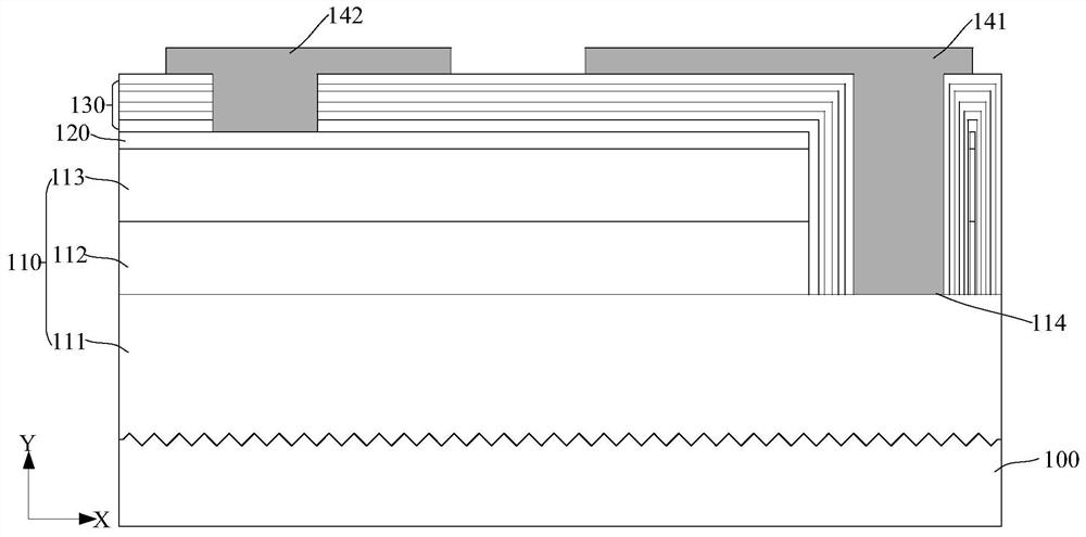
[0068] This embodiment provides a flip-chip semiconductor light-emitting element, such as figure 2 As shown, the semiconductor light emitting element of this embodiment includes a substrate 100, a light emitting epitaxial layer 110 formed on the substrate, and the light emitting epitaxial layer 110 includes a first conductivity type semiconductor layer 111, an active layer formed on the substrate 100 in sequence, layer 112 and the second conductivity type semiconductor layer 113 .

[0069] In this embodiment, the substrate 100 may be an insulating substrate. The substrate 100 may be a growth substrate for growing the light-emitting epitaxial layer 110 , for example, including a sapphire substrate. Such as figure 2 As shown, the substrate 100 further includes a plurality of protrusions formed on at least a part of the upper surface thereof. The plurality of protrusions of the substrate 100 may be formed in regular and / or irregular patterns. For example, the substrate 100 ...

Embodiment 2

[0085] This embodiment also provides a flip-chip semiconductor light-emitting element, and the similarities with the semiconductor light-emitting element provided in Embodiment 1 will not be repeated, but the difference lies in:

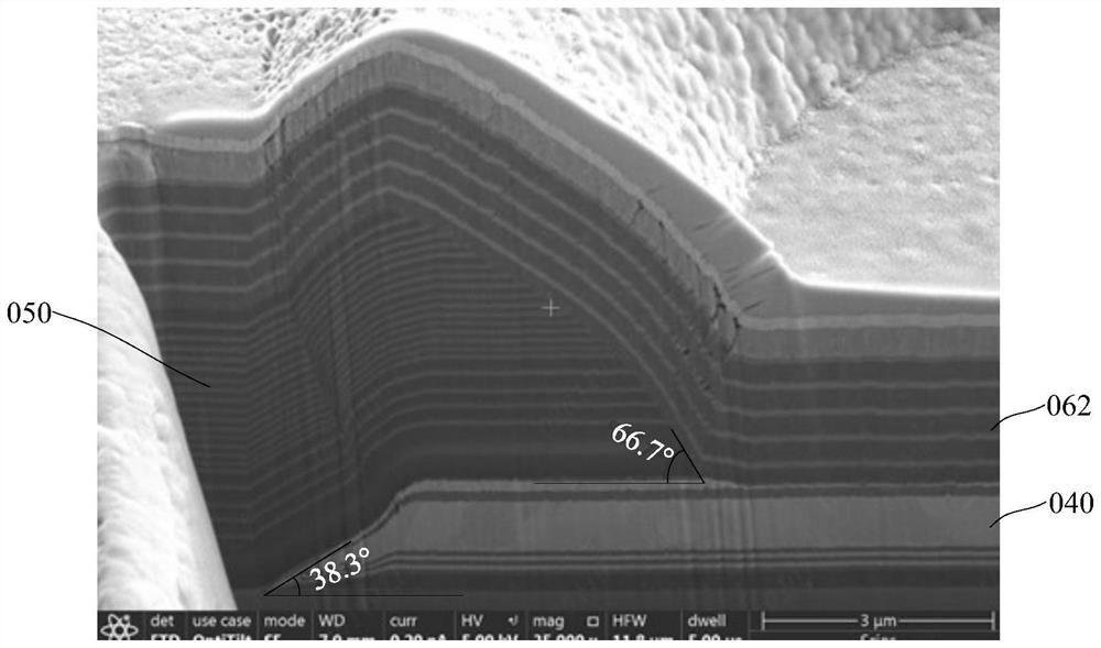
[0086] In this embodiment, the insulating layer 130 further includes a third insulating protective layer, wherein the third insulating protective layer is interposed between the first insulating protective layer and the insulating reflective layer, and the third insulating protective layer has a high density It is better than the compactness of the insulating reflective layer, but lower than that of the first insulating protective layer. The first insulating layer is obtained by ALD deposition, for example, an aluminum oxide layer, and the third insulating protection layer is obtained by PECVD deposition, such as a silicon oxide layer, and the thickness of the third insulating protection layer is between 80nm and 450nm. More preferably, the thickness...

Embodiment 3

[0088] This embodiment also provides a flip-chip semiconductor light-emitting element, and the similarities with the semiconductor light-emitting element provided in Embodiment 1 will not be repeated, but the difference lies in:

[0089] The insulating layer 130 in this embodiment includes a fourth insulating protective layer, wherein the fourth insulating protective layer is between the second insulating protective layer and the insulating reflective layer, and the density of the fourth insulating protective layer is higher than that of the insulating reflective layer. The density of the layer is lower than that of the second insulating protective layer. The second insulating layer is obtained by ALD deposition, such as an aluminum oxide layer, and the fourth insulating protective layer is obtained by a PECVD deposition process, such as a silicon oxide layer or a silicon nitride layer. Preferably, the thickness of the second insulating protective layer is between In 8nm-200nm...


PUM

PropertyMeasurementUnit
thicknessaaaaaaaaaa
thicknessaaaaaaaaaa
thicknessaaaaaaaaaa

Abstract

The invention provides a flip semiconductor light-emitting element, a semiconductor light-emitting device and a display device. The semiconductor light-emitting element comprises a substrate and a light-emitting epitaxial layer formed on the substrate. When an electrode structure is formed above the light-emitting epitaxial layer, a first electrode layer partially covering the light-emitting epitaxial layer above the light-emitting epitaxial layer is omitted, so that the surface of the light-emitting epitaxial layer is relatively high in flatness. When an insulating reflection layer and an insulating protection layer are formed subsequently, the flatness of the insulating reflection layer and the insulating protection layer can be ensured. Moreover, the overall thickness of the insulating reflection layer and the insulating protection layer is not greater than 3 microns, so that abnormal protrusions cannot occur when the electrode through holes are formed in the insulating reflection layer and the insulating protection layer, the electrode through holes have good morphology, the adhesion of a subsequently formed electrode bonding pad in the electrode through hole and the adhesion of the subsequently formed electrode bonding pad above the insulating protection layer are enhanced, and the electrode bonding pad does not have defects such as cracks or fractures, so that the stability and reliability of the device are enhanced.

Description

technical field [0001] The invention relates to the field of semiconductor devices, in particular to a flip-chip semiconductor light emitting element, a semiconductor light emitting device and a display device. Background technique [0002] Semiconductor light-emitting elements, or light-emitting diodes, are widely used in various products such as large backlight units, general lighting, and electrical components. Micro-light-emitting diodes (Mini LEDs) are especially favored in the field of display panels due to their advantages of small size, high light source utilization rate, and long life. [0003] With the continuous reduction of mini LED size, the design of chip graphics has higher and more stringent requirements for line width. In the current mini LED manufacturing process, a first electrode layer will be formed above the epitaxial layer. The first electrode layer does not completely cover the epitaxial layer, and will form a similar step structure above the epitaxi...

Claims


Application Information

Patent Timeline
Patent Type & Authority Applications(China)
IPC IPC(8): H01L33/36H01L33/44H01L33/46H01L33/14H01L33/48H01L33/62H01L27/15
CPCH01L33/44H01L33/46H01L33/36H01L33/14H01L33/48H01L33/62H01L27/156H01L33/382H01L33/10
Inventor 黄敏夏章艮詹宇林素慧何安和张中英
Owner XIAMEN SANAN OPTOELECTRONICS CO LTD
Why Eureka
Try Eureka