Longitudinal BCD device capable of inhibiting parasitism and preparation method thereof
A device and vertical technology, which is applied in the field of vertical BCD devices and its preparation, can solve the problems of large area occupied by DMOSFET drain area, large on-resistance, and poor compatibility of VDMOSFET, so as to improve chip utilization, reduce on-resistance, The effect of reducing chip area
- Summary
- Abstract
- Description
- Claims
- Application Information
AI Technical Summary
Problems solved by technology
Method used
Image
Examples
Embodiment 1
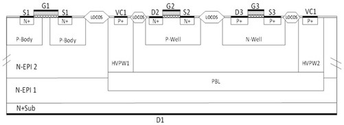
[0059] figure 1 Shown is a schematic structural diagram of a vertical BCD integrated device. Taking an N-type planar VDMOSFET device as an example, it can also be a VDMOSFET device with a trench or super junction structure. The vertical BCD device can reduce the on-resistance and reduce the chip area. , However, it also has a defect at the same time, the voltage added to the drain of the VDMOSFET will also affect the CMOS device in the BCD device. Therefore, a P-well needs to be added to isolate the CMOS devices. Since the deep P-well HVPW is used alone to realize the well, the well is deep and requires high process capability and precision. Due to the limitation of machine capacity, the depth of HVPW can be reduced by making P-type buried layer PBL, and the corresponding process is easier to realize. In addition, the concentration of PBL in the buried layer can be adjusted, and increasing the concentration of PBL can effectively inhibit the conduction of the parasitic tube ...
Embodiment 2
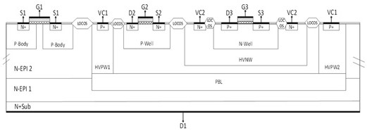
[0084] Figure 11 Vertical BCD devices shown in the figure 1 On the basis of the structure, a layer of HVNW deep N-type well is added. The main function is to prevent the reverse breakdown of the diode formed between the N-Well of PMOS and HVPW in CMOS, which will affect the normal operation of PMOS. Since N-Well is mainly used to adjust the channel parameters of PMOS, at the same time, it is difficult to take into account the reverse withstand voltage of HVPW. Therefore, it is necessary to add a layer of HVNW deep N well to adjust the reverse of the diode formed between HVPW and HVPW. The reverse withstand voltage must be greater than the breakdown withstand voltage of the PMOS. In the figure, VC2 is the lead-out end of the HVNW.
[0085] The specific structure of the vertical BCD device in this embodiment is as follows, including:
[0086] N-type substrate,
[0087] The first N-type epitaxial layer formed on the upper surface of the N-type substrate, the first N-type epit...
PUM
| Property | Measurement | Unit |
|---|---|---|
| thickness | aaaaa | aaaaa |
Abstract
Description
Claims
Application Information
 - R&D Engineer
- R&D Manager
- IP Professional
- Industry Leading Data Capabilities
- Powerful AI technology
- Patent DNA Extraction
Browse by: Latest US Patents, China's latest patents, Technical Efficacy Thesaurus, Application Domain, Technology Topic, Popular Technical Reports.
© 2024 PatSnap. All rights reserved.Legal|Privacy policy|Modern Slavery Act Transparency Statement|Sitemap|About US| Contact US: help@patsnap.com


