Semiconductor gas sensor and automatic packaging method thereof

A gas sensor and packaging method technology, which is applied in the fields of gaseous chemical plating, decorative arts, microstructure devices, etc., can solve the problems of easy leakage, blocked ventilation holes of protective caps, low packaging accuracy, etc., and achieves improved detection accuracy and packaging. Fast and efficient, good electrical connection performance

Active Publication Date: 2021-11-30
河南森斯科传感技术有限公司
View PDF5 Cites 4 Cited by
  • Summary
  • Abstract
  • Description
  • Claims
  • Application Information

AI Technical Summary

Problems solved by technology

This packaging method is not fast enough and accurate, and the packaging is difficult and prone to leakage
[0004] At this stage, the air holes of the semiconductor gas sensor protective cap are prone to blockage, and the shock absorption effect is poor. It is easy to cause damage to the internal detection components and heating components when the device is shaken. The dynamic response and static response of semiconductor gas sensors will affect, and will also interfere with the recovery time of semiconductor gas sensors, so that the accuracy of detection cannot be guaranteed. At the same time, the packaging of semiconductor gas sensors is difficult and the packaging accuracy is low

Method used


Image

  • Semiconductor gas sensor and automatic packaging method thereof
  • Semiconductor gas sensor and automatic packaging method thereof
  • Semiconductor gas sensor and automatic packaging method thereof

Examples


no. 1 example

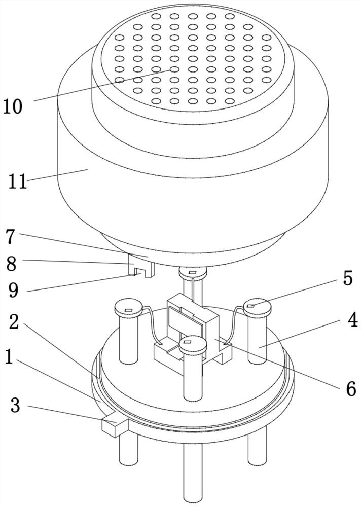
[0034] Such as Figure 1-4 , a semiconductor gas sensor, comprising a tube base 1, a plurality of groups of terminal posts 4 are plugged in a uniform array inside the tube base 1, the terminal posts 4 are located at the bottom part of the tube base 1 and connected to an alarm, and the top of the tube base 1 is provided with The substrate holder 19 can be packaged on the top of the tube holder 1 by automatic packaging methods such as solid crystal and wire bonding. The top of the substrate holder 19 is provided with a gas sensor unit 6, and the monitoring of the gas is realized through the gas sensor unit 6. The tube holder The top of 1 is sleeved with a protective cap 7, and the protective cap 7 protects the internal structure.

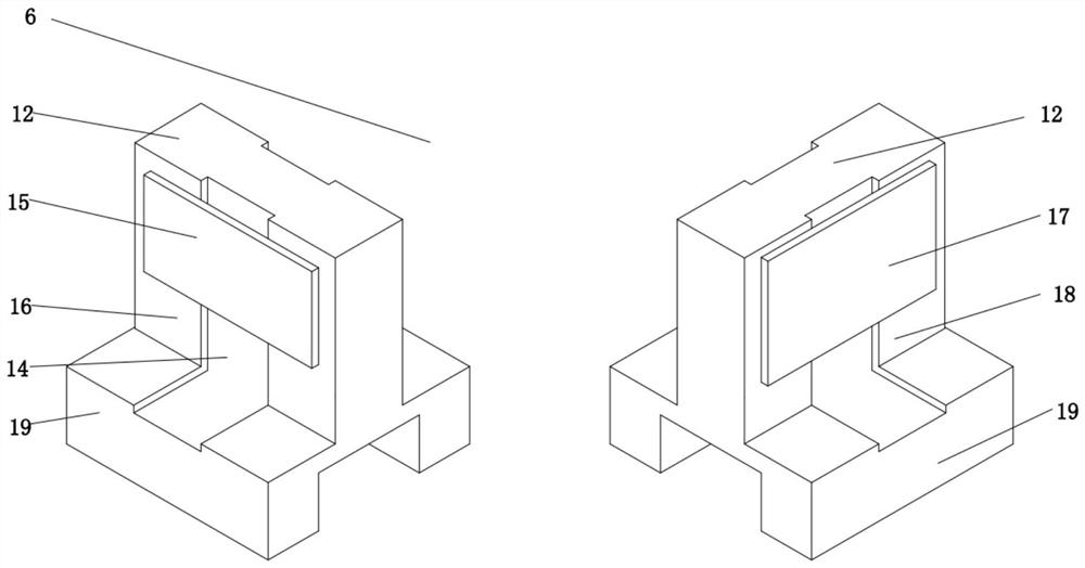
[0035]Gas-sensitive unit 6 comprises substrate sheet 12, and substrate holder 19 and substrate sheet 12 are all good heat insulating properties and the material of high temperature resistance, as quartz, and substrate holder 19 is " U " shape, and sub...

no. 2 example

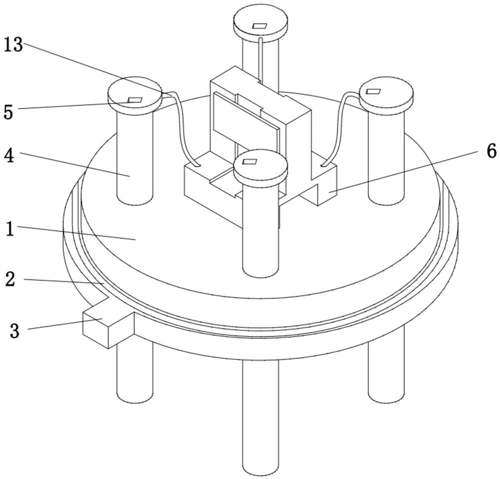
[0041] Such as Figure 5 with Image 6 , based on a semiconductor gas sensor provided in the first embodiment, in actual use, due to problems such as vibration in the environment, the structure inside the protective cap 7 will be damaged, and the detection effect of the gas sensitive material 15 is the same as that of the gas When the flow rate of the detection gas reaches the position of the gas-sensitive material 15 through the vent hole 10, the flow rate is too large or too small, which will affect the detection results. Generally, the flow rate of the detection gas is preferably 500-1000 sccm, and, In order to make the measurement accuracy of the semiconductor gas sensor higher, the gas flow rate flowing through the sensor should be kept constant as much as possible. In order to solve the above problems, improve the anti-seismic efficiency and assembly efficiency of the device, and ensure that the flow rate of the detected gas is stable and controllable, the semiconductor ...

no. 3 example

[0051] Such as Figure 7 , based on the semiconductor gas sensor provided in the second embodiment, in order to ensure the fast, accurate and tightness of the package in actual packaging, it is necessary to carry out reasonable packaging program planning and arrangement according to the actual operation situation, so this embodiment provides a Automated packaging method for semiconductor gas sensors:

[0052] S1. Make a patterned metal electrode on the top of the substrate holder 19 by using a coating method, wherein the coating process mainly includes evaporation, sputtering, electroplating or screen printing, and the metal electrode can be made of gold or platinum;

[0053] S2. Make a deep groove 14 on the top of the substrate holder 19 through a groove-making process, wherein the groove-making process mainly includes precision cutting, corrosion or sandblasting;

[0054] S3. Use the blue film to fix and cut the substrate seat 19, and then expand the film to form a U-shaped...


PUM


Abstract

The invention belongs to the technical field of sensor packaging, and particularly relates to a semiconductor gas sensor which comprises a tube socket. A plurality of groups of binding posts are uniformly inserted in the tube socket in an array manner, insertion grooves are formed in the tops of the binding posts, a plurality of groups of gas outlet holes are uniformly formed in the bottom of the interior of the tube socket in an array manner, and a substrate seat is arranged at the top of the tube socket. A gas sensitive unit is arranged at the top of the substrate seat, and the top of the tube socket is sleeved with a protective cap; the gas sensitive unit comprises a substrate sheet, one side of the substrate sheet is provided with a gas sensitive electrode, the other side of the gas sensitive electrode is provided with a gas sensitive material, and the other side of the substrate sheet is provided with a heating electrode. The device not only can provide a very good temperature environment for the gas sensitive material, but also can play a role in damping and buffering and protecting the internal structure, the flow rate of gas flowing to the gas sensitive material can be controlled, the adaptability and the detection accuracy of the device are improved, and the packaging method provided by the invention is rapid, accurate, stable and effective.

Description

technical field [0001] The invention belongs to the technical field of sensor packaging, in particular to a semiconductor gas sensor and an automatic packaging method thereof. Background technique [0002] Semiconductor gas sensor is a gas sensor that uses semiconductor gas sensor as a sensitive element. It is the most common gas sensor and is widely used in combustible gas leakage detection devices in homes and factories. It is suitable for the detection of methane, liquefied petroleum gas, hydrogen, etc.; semiconductor gas The sensor is made by using the redox reaction of gas on the surface of the semiconductor to cause the resistance value of the sensitive element to change. When the semiconductor device is heated to a stable state, when the gas contacts the semiconductor surface and is adsorbed, the adsorbed molecules first diffuse freely on the surface of the object, lose kinetic energy, part of the molecules are evaporated, and the other part of the remaining molecules...

Claims


Application Information

Patent Timeline
Patent Type & Authority Applications(China)
IPC IPC(8): G01N27/12B81C1/00H05B3/06
Inventor 时学瑞王冉申林贾毅博韩毓
Owner 河南森斯科传感技术有限公司
Why Eureka
Try Eureka