Process for manufacturing three-dimensional circuit through laser etching and plastic surface carbonization

A laser etching and surface fabrication technology, applied in the field of circuit manufacturing, can solve problems such as difficulty in meeting high-standard manufacturing requirements for mobile phone antennas, complex laser parameter debugging, and reduced laser processing efficiency, achieving good toughness, improved yield, and injection molding cracks. low risk effect

Pending Publication Date: 2021-12-10
SHANGHAI SHENZHI OPTOELECTRONICS TECH CO LTD
View PDF0 Cites 2 Cited by
  • Summary
  • Abstract
  • Description
  • Claims
  • Application Information

AI Technical Summary

Problems solved by technology

[0011] Aiming at the deficiencies of the prior art, the present invention provides a process for making three-dimensional lines by laser etching and carbonizing the plastic surface, which solves the problem of equipment and material costs in the LDS process and the reduction in toughness caused by the addition of modified components to the material. Plastic parts are easy to cracking problem
Our new three-dimensional circuit manufacturing process also effectively solves the related problems of the LAP process: complex laser parameter debugging, long proofing cycle; poor mass production stability, low yield rate, and it is difficult to meet the high standard manufacturing requirements of the mobile phone antenna industry; In order to improve Subsequent coating performance and coating adhesion laser scanning often need to cross two filling scanning methods, resulting in a significant reduction in laser processing efficiency

Method used


Image

  • Process for manufacturing three-dimensional circuit through laser etching and plastic surface carbonization
  • Process for manufacturing three-dimensional circuit through laser etching and plastic surface carbonization
  • Process for manufacturing three-dimensional circuit through laser etching and plastic surface carbonization

Examples


Embodiment

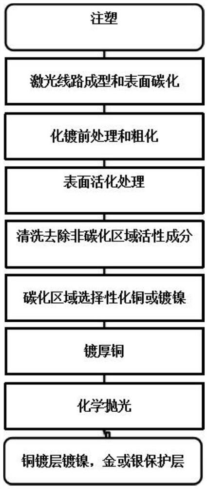
[0064] Such as Figure 1-9 As shown, the embodiment of the present invention provides a process for making a three-dimensional circuit by laser etching and carbonizing the plastic surface, including the following specific steps:

[0065] S1. The plastic substrate carrying the circuit is made by injection molding. The plastic body is often not only the carrier of the circuit but also the structural component of the product design. Because of this, this process can provide great flexibility for product design. In order to ensure the subsequent plating effect, different injection molding materials need to use different combinations of laser parameters according to the actual effect, and the roughening potion and process parameters during chemical roughening also need to make necessary adjustments;

[0066] S2. The graphics of the circuit is processed on the surface of the plastic part by laser engraving, and the carbonization effect of the circuit area on the plastic surface is r...


PUM


Abstract

The invention provides a process for manufacturing a three-dimensional circuit through laser etching, plastic surface carbonization and chemical plating, and relates to the technical field of manufacturing of circuits on plastic surfaces. The process comprises the following specific steps that a plastic substrate for bearing the circuit is manufactured through injection molding; a pattern of the circuit is processed on the surface of a plastic part in a laser engraving mode, and the full carbonization effect of a circuit area on the surface of the plastic part is achieved through reasonable selection of a laser light source and optimization of laser parameters while laser is used for processing the circuit; metal is plated in the laser carbonization area through subsequent chemical plating, so that the metal circuit is manufactured on the surface of the plastic; and when the circuit is manufactured on the first-level appearance surface, the smoothness of a plating layer can be fully improved in combination with an optimized special treatment means, and the size of a step between the plating layer and the plastic is reduced, so that the subsequent spraying cost is greatly reduced.

Description

technical field [0001] The invention relates to the technical field of manufacturing circuits on plastic surfaces, in particular to a process for manufacturing three-dimensional circuits by laser etching and carbonizing plastic surfaces. Background technique [0002] LDS (LASER DIRECT STRUCTURING, Laser Direct Structuring) is a manufacturing process that adds special metal complexes to plastic particles, and then creates three-dimensional circuits on the surface of plastic structural parts by laser molding. This process was invented by German LPK, because it can be highly integrated in antenna design and manufacturing, saves space and is convenient for antenna design and routing, so it has a very good reputation in the field of antenna manufacturing for smartphones and wearable devices. Application prospects. However, due to the patent threshold of LPK, the plastic particles used in this production process are expensive, and the laser equipment is required to use German LPK...

Claims


Application Information

Patent Timeline
Patent Type & Authority Applications(China)
IPC IPC(8): B23K26/362B23K26/70B23K26/402
CPCB23K26/362B23K26/702B23K26/402B23K2103/42
Inventor 陈设刘强高兆勇
Owner SHANGHAI SHENZHI OPTOELECTRONICS TECH CO LTD
Why Eureka
Try Eureka