Involute laser-assisted wafer cutting processing method and system and stress detection method

A laser-assisted cutting processing technology, applied in laser welding equipment, metal processing equipment, welding/welding/cutting items, etc., can solve the problems of large residual stress and high roughness of the incision, achieve low residual stress and improve detection speed and stability, smooth cut

Active Publication Date: 2021-12-10
PEKING UNIV
View PDF11 Cites 0 Cited by
  • Summary
  • Abstract
  • Description
  • Claims
  • Application Information

AI Technical Summary

Problems solved by technology

[0007] Embodiments of the present invention provide an involute laser-assisted wafer cutting processing method, system, and

Method used


Image

  • Involute laser-assisted wafer cutting processing method and system and stress detection method
  • Involute laser-assisted wafer cutting processing method and system and stress detection method
  • Involute laser-assisted wafer cutting processing method and system and stress detection method

Examples


Example Embodiment

[0057] In order to make the purpose, technical solution and advantages of the present application clearer, the present application will be further described in detail below in conjunction with the accompanying drawings and embodiments. It should be understood that the specific embodiments described here are only used to explain the present application, and are not intended to limit the present application.

[0058] In the description of the present invention, unless otherwise stated, the terms "comprising", "having" and any variations thereof are intended to cover a non-exclusive inclusion, for example, a process, method, system, Products or equipment are not necessarily limited to those steps or units that have been explicitly listed, but may also include other steps or units that are not explicitly listed but inherent to these processes, methods, products or equipment, or further The steps or units added by the optimization scheme.

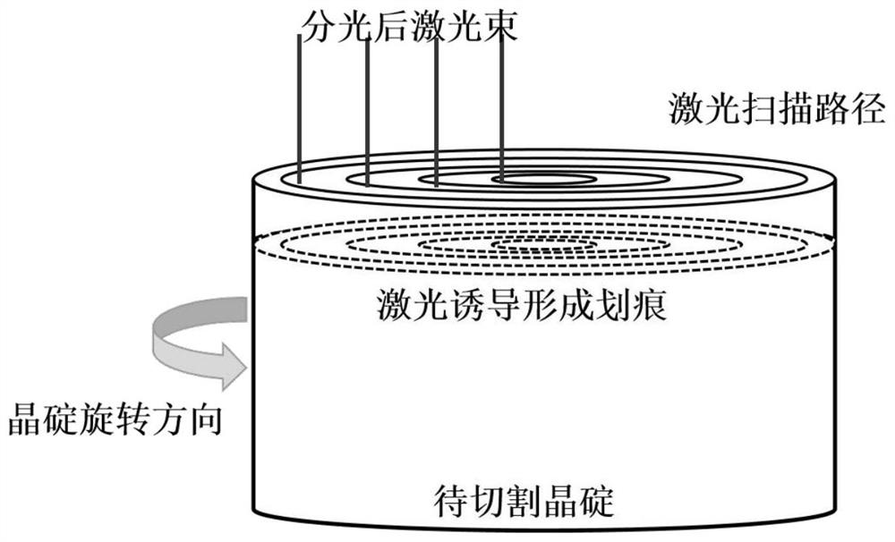
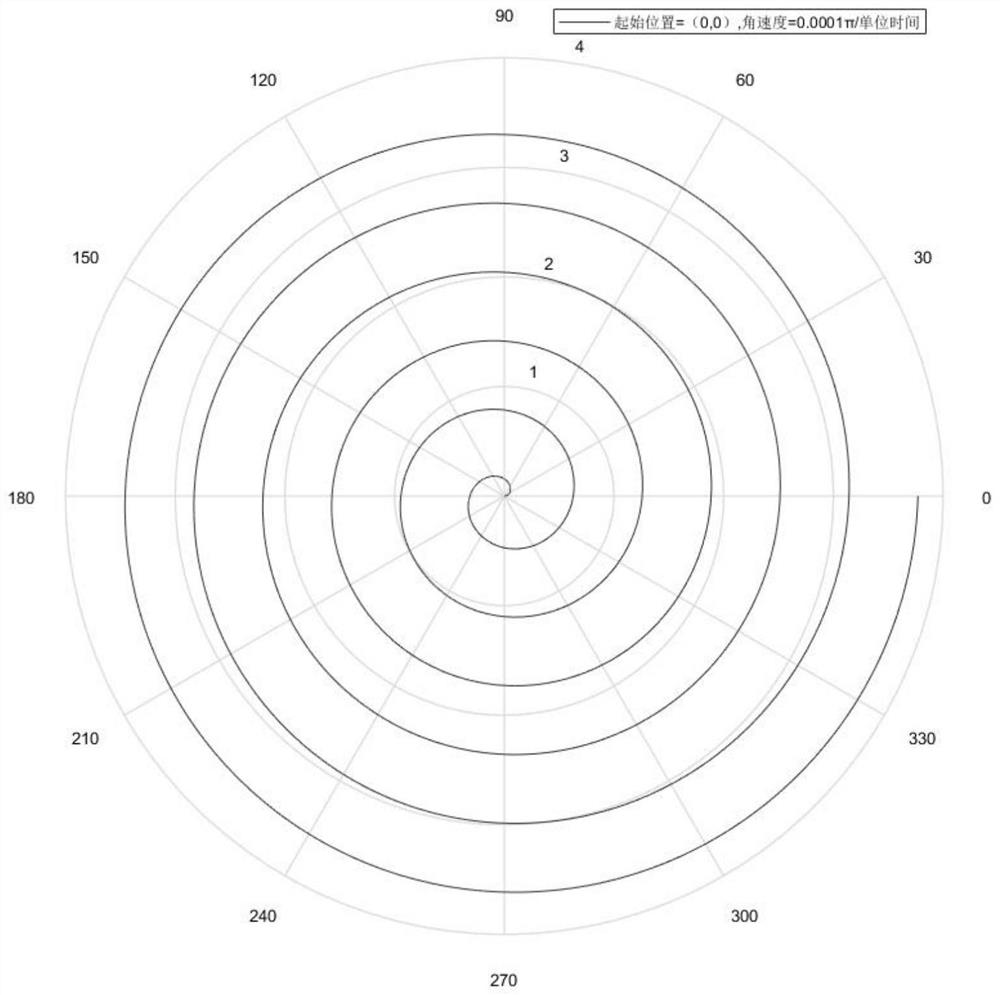
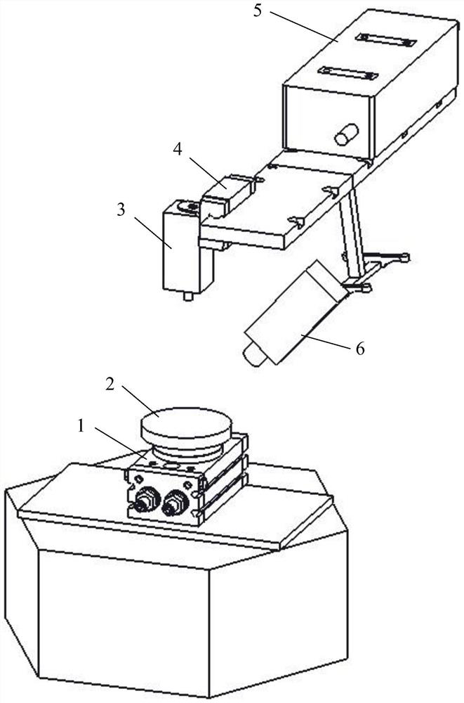
[0059] An embodiment of the present inve...


PUM


Abstract

The invention discloses an involute laser-assisted wafer cutting processing method and system and a stress detection method, which are used for overcoming the defects of high roughness and large residual stress at a notch in the prior art. The method comprises the following steps of fixing a wafer on a rotary table, and placing the rotary table on an objective table; adjusting the position of the objective table on an X-Y plane, so that a laser is focused at the center of the wafer; driving the rotary table to rotate at a constant speed, and driving the laser to horizontally move at a constant speed along the X axis or the Y axis, so that the motion curve of laser on the wafer is an involute; and controlling the peak energy and the pulse width of the laser pulse in the uniform motion process of the laser, so that the wafer is cut. According to the involute laser-assisted wafer cutting processing method and system and the stress detection method provided by the invention, the machining speed is higher and more stable, the implosion position is more accurate, a product notch is smoother, and residual stress is lower.

Description

technical field [0001] The invention relates to the field of wafer cutting technology, in particular to an ultrafast laser wafer cutting processing method, system and stress detection method. Background technique [0002] Wide bandgap semiconductors have the advantages of large bandgap width, high electron saturation drift velocity, and strong breakdown field. They are ideal materials for the preparation of high power density, high frequency, and low loss electronic devices. Silicon carbide (SiC) materials have the advantages of high thermal conductivity, good chemical stability, and high temperature resistance. Epitaxial wide-bandgap semiconductor materials on SiC substrates can give full play to the advantages of wide-bandgap semiconductor materials and improve wide-bandgap semiconductor materials. The performance of semiconductor electronic devices is of great importance. But because SiC has very high hardness, more advanced cutting technology is required to obtain large...

Claims


Application Information

Patent Timeline
IPC IPC(8): B23K26/38B23K26/402B23K26/082G01N21/65G01L1/24
CPCB23K26/38B23K26/402B23K26/082G01N21/65G01L1/24B23K2103/56
Inventor 王振宇王添瑜李娟
Owner PEKING UNIV
Why Eureka
Try Eureka