
Processor element for quantum information processor

A technology of processor elements and quantum dots, applied in the fields of nanotechnology, electrical components, semiconductor devices for information processing, etc., can solve the problems of speeding up processing time, high precision obstacles, etc., to achieve the effect of easy manufacturing

Pending Publication Date: 2021-12-21
QUANTUM MOTION TECH LTD
View PDF0 Cites 0 Cited by
  • Summary
  • Abstract
  • Description
  • Claims
  • Application Information

AI Technical Summary

Problems solved by technology

[0005] Universal quantum computers promise to speed up processing times for several operations, such as factorization of large numbers, search algorithms, and quantum simulations, but progress in the development of such quantum computers has been hampered by the high precision required for the control of quantum states, and the need to scale quantum computers to Difficulties in being able to handle large numbers of qubits or qubits

Method used


Image

  • Processor element for quantum information processor
  • Processor element for quantum information processor
  • Processor element for quantum information processor

Examples


Embodiment Construction

[0048] Although different embodiments are described below, the invention is not limited to these embodiments and variations from these embodiments may well fall within the scope of the invention, which is limited only by the appended claims.

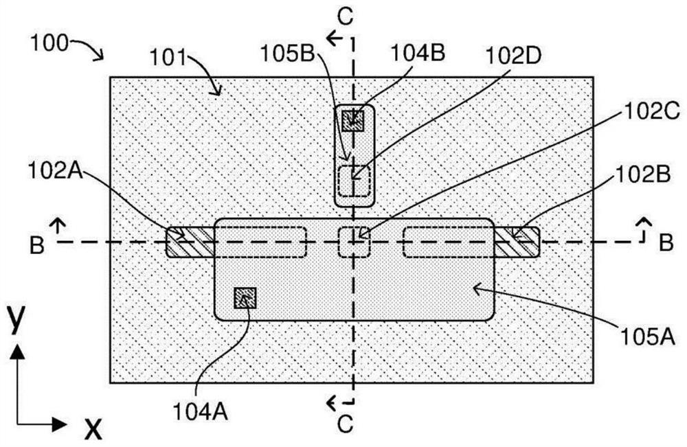
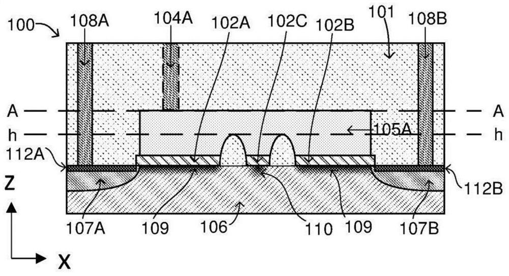
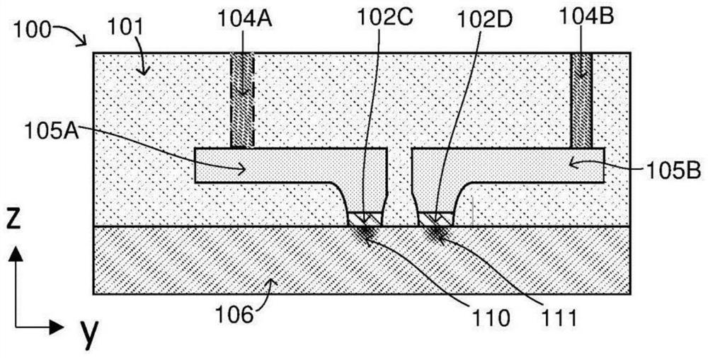
[0049] Figure 1A-Figure 1C A processor element 100 is depicted according to an example. Figure 1A A cross-sectional view of the processor element 100 in the x-y plane at a first height along the z-axis is shown. That is, FIG. 1 illustrates processor element 100 as viewed from above (plan view) at a first height within processor element 100 . Specifically, the plan is at Figure 1B at the height indicated by line A in Figure 1B shows generally along the direction B ( Figure 1A A cross-sectional view of processor element 100 as viewed in ). Figure 1B The source and drain electrodes are not in Figure 1A shown in . Figure 1C show roughly along the direction C ( Figure 1A A second cross-sectional view of processor element 100 as v...


PUM

PropertyMeasurementUnit
thicknessaaaaaaaaaa
thicknessaaaaaaaaaa
sizeaaaaaaaaaa

Abstract

Processor elements are described herein. A processor element comprises a silicon layer. The processor element further comprises one or more conductive electrodes. The processor element further comprises dielectric material having a non-uniform thickness, the dielectric material disposed at least between the silicon layer and the one or more conductive electrodes. In use, when a bias potential is applied to one or more of the conductive electrodes, the positioning of the one or more conductive electrodes and the non-uniform thickness of the dielectric material together define an electric field profile to induce a quantum dot at an interface between the silicon layer and the dielectric layer. Methods are also described herein.

Description

technical field [0001] The present disclosure relates to processor elements for quantum information processing. In particular, the application relates to processor elements that use confinement regions, such as quantum dots, etc. to store charge carriers serving as qubits, and that can be fabricated by complementary metal-oxide-semiconductor fabrication processes . Background technique [0002] The invention described herein is based at least in part on quantum mechanics, quantum information and quantum computing. For the interested reader, the basic principles are described in detail in "Quantum Computation and Quantum Information" by Michael ANielsen and Isac L Chuang. In particular, this reference covers the properties of qubits and the fundamentals of quantum measurements on complementary bases, and provides an introduction to quantum error correction and fault-tolerant quantum computing. This reference also acquaints the reader with notations that are routinely used ...

Claims


Application Information

Patent Timeline
Patent Type & Authority Applications(China)
IPC IPC(8): H01L29/76H01L21/335G06N10/00
CPCH01L29/7613H01L29/66439G06N10/00B82Y10/00H01L29/66977H01L29/66984H01L29/0673H01L29/0653H01L29/4232H01L29/42368G06N10/40
Inventor 迈克尔·福加蒂马修·肖曼斯约翰·莫顿
Owner QUANTUM MOTION TECH LTD
Learn More