Gallium nitride normally-off device with mixed gate electrode structure and preparation method of gallium nitride normally-off device

A gate electrode, normally-off technology, which is applied in the field of gallium nitride normally-off devices and its preparation, can solve the problem of not being able to meet the gate electrode threshold voltage requirements, and achieve the effects of improving long-term reliability and increasing switching frequency.

Pending Publication Date: 2021-12-24
宁波铼微半导体有限公司
View PDF0 Cites 1 Cited by
  • Summary
  • Abstract
  • Description
  • Claims
  • Application Information

AI Technical Summary

Problems solved by technology

[0004] However, at present, the threshold voltage of the gate electrode of the P-GaN cap layer high electron mobility transistor (HEMT) is maintained at about 2V, which cannot meet the requirements for the threshold voltage of the gate electrode in actual operation.

Method used


Image

  • Gallium nitride normally-off device with mixed gate electrode structure and preparation method of gallium nitride normally-off device
  • Gallium nitride normally-off device with mixed gate electrode structure and preparation method of gallium nitride normally-off device
  • Gallium nitride normally-off device with mixed gate electrode structure and preparation method of gallium nitride normally-off device

Examples


Embodiment 1

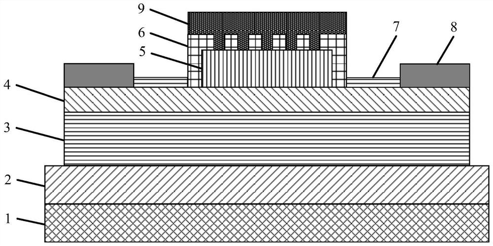
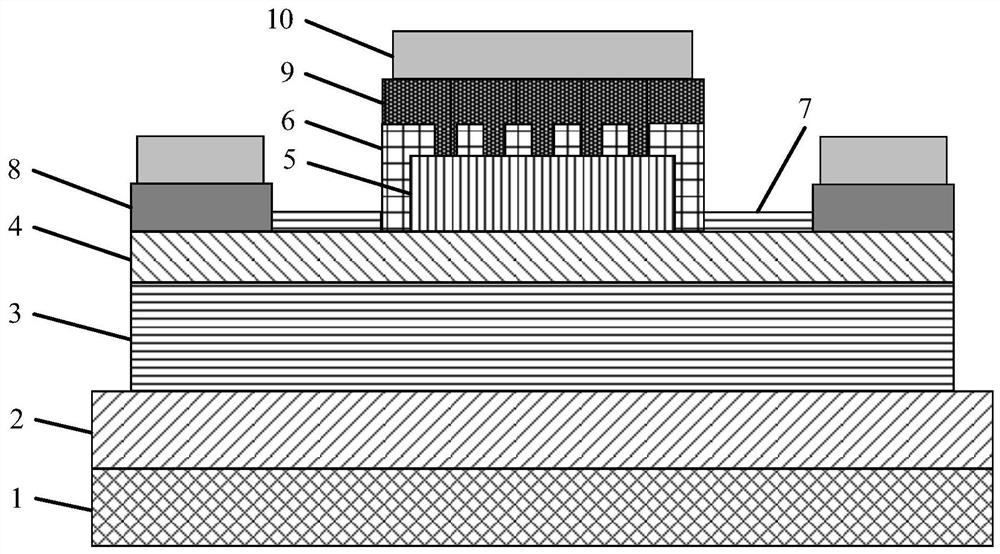
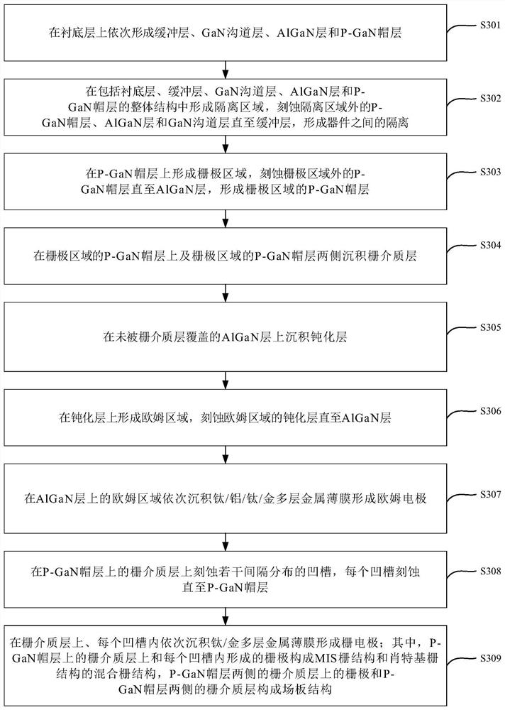
[0042] In order to increase the threshold voltage of the device, an embodiment of the present invention proposes a gallium nitride normally-off device with a mixed gate electrode structure, please refer to figure 1 , figure 1 It is a schematic structural diagram of a gallium nitride normally-off device with a hybrid gate electrode structure provided by an embodiment of the present invention, and the device includes:

[0043] substrate layer 1;

[0044] A buffer layer 2, a GaN channel layer 3 and an AlGaN layer 4 disposed on the substrate layer 1 in sequence;

[0045] The P-GaN cap layer 5 and two ohmic electrodes 8 arranged on the AlGaN layer 4; wherein, the two ohmic electrodes 8 are respectively arranged on both ends of the upper surface of the AlGaN layer 4, and the P-GaN cap layer 5 is arranged on two ohmic electrodes. between the electrodes 8;

[0046] Be arranged on the P-GaN cap layer 5 and the gate dielectric layer 6 on both sides of the P-GaN cap layer 5; wherein, ...


PUM

PropertyMeasurementUnit
thicknessaaaaaaaaaa
thicknessaaaaaaaaaa
widthaaaaaaaaaa

Abstract

The invention discloses a gallium nitride normally-off device with a mixed gate electrode structure and a preparation method of the gallium nitride normally-off device. The gallium nitride normally-off device comprises a buffer layer, a GaN channel layer, an AlGaN layer and a P-GaN cap layer which are sequentially arranged on a substrate layer, two ohmic electrodes which are arranged on the AlGaN layer, gate dielectric layers which are arranged on the P-GaN cap layer and on the two sides of the P-GaN cap layer, a passivation layer which is arranged on the AlGaN layer between the ohmic electrode and the gate dielectric layer on the two sides of the P-GaN cap layer, and a gate electrode which is arranged on the gate dielectric layer and filled in the groove of the gate dielectric layer. The gate electrode on the gate dielectric layer on the P-GaN cap layer and the gate electrodes filled in the plurality of grooves form a mixed gate structure of an MIS gate electrode structure and a Schottky gate electrode structure; and the gate electrodes on the gate dielectric layers on the two sides of the P-GaN cap layer and the gate dielectric layers on the two sides of the P-GaN cap layer form a field plate structure. The threshold voltage of the gate electrode of the device is improved, the switching frequency of the device is improved, and meanwhile the long-term reliability of the gate electrode of the device is improved.

Description

technical field [0001] The invention belongs to the technical field of semiconductor power devices, and in particular relates to a gallium nitride normally-off device with a mixed gate electrode structure and a preparation method thereof. Background technique [0002] Wide-bandgap semiconductor materials represented by gallium nitride (GaN) have a high critical breakdown electric field, which can achieve lower capacitance and on-resistance at the same breakdown voltage, and are recognized as next-generation power device materials. Therefore, the development of gallium nitride (GaN) power devices to replace traditional silicon (Si)-based devices is a key means to improve power utilization efficiency and alleviate the energy crisis, and is expected to play a pivotal role in emerging markets. As a representative device of gallium nitride (GaN), a high electron mobility transistor (HEMT) based on an AlGaN / GaN epitaxial structure, due to its unique high mobility two-dimensional e...

Claims


Application Information

Patent Timeline
Patent Type & Authority Applications(China)
IPC IPC(8): H01L29/778H01L29/423H01L29/40H01L29/45H01L21/335
CPCH01L29/66462H01L29/7783H01L29/402H01L29/42356H01L29/452
Inventor 蒲涛飞李柳暗敖金平
Owner 宁波铼微半导体有限公司
Why Eureka
Try Eureka