Operational amplifier circuit offset voltage calibration method, device thereof and system

A technology of operational amplifier circuit and offset voltage, applied in improving amplifiers to reduce temperature/power supply voltage changes, improving amplifiers to reduce nonlinear distortion, improving amplifier input/output impedance, etc., can solve the compromise between compensation accuracy and area , a large number of voltage divider resistors, offset voltage elimination and other issues, to achieve the effect of reducing the number, improving linearity, and reducing the occupied area

Pending Publication Date: 2022-01-07
NINGBO CRRC TIMES TRANSDUCER TECH CO LTD
View PDF0 Cites 4 Cited by
  • Summary
  • Abstract
  • Description
  • Claims
  • Application Information

AI Technical Summary

Problems solved by technology

Among them, the mismatch of the operational amplifier itself can be eliminated by Chopper technology or Correlated Double Sampling (CDS related double sampling) technology to the range required by the index, and the ratio mismatch of resistor resistance / capacitance is mainly caused by process deviation. The offset voltage cannot be eliminated by inherent technology, and the offset voltage can only be reduced by means of trimming.
[0003] The traditional method of trimming the ratio mismatch of the resistance value / capacitance value of the operational amplifier is a binary current compensation scheme, that is, the ratio mismatch of the resistance value / capacitance value is corrected by a compensation circuit composed of a voltage divider For trimming, in order to achieve the required compensation accuracy, a large number of voltage divider resistors are required, resulting in a large circuit area, and a compromise between compensation accuracy and area is required, and the compensation accuracy is limited

Method used


Image

  • Operational amplifier circuit offset voltage calibration method, device thereof and system
  • Operational amplifier circuit offset voltage calibration method, device thereof and system
  • Operational amplifier circuit offset voltage calibration method, device thereof and system

Examples


Embodiment 1

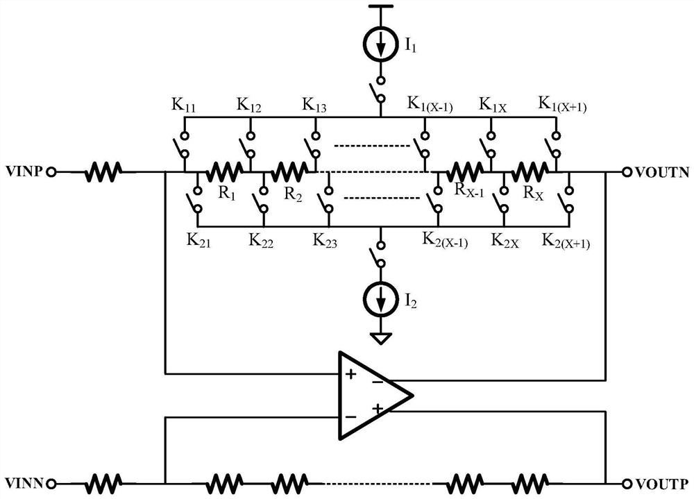
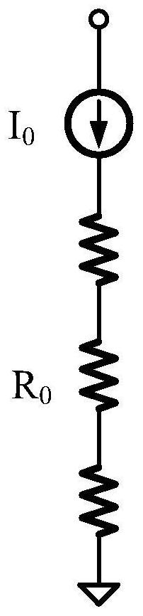
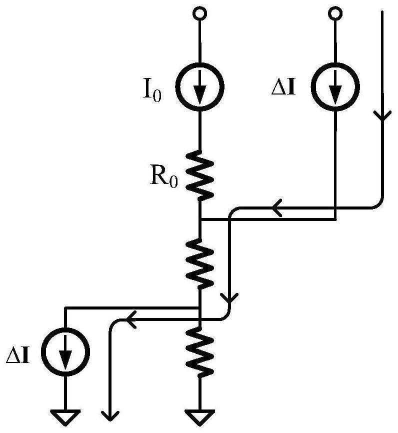
[0060] figure 1 A circuit diagram of a compensation circuit provided in the embodiment of the present application; figure 2 Simplified circuit schematic diagram without calibration; image 3 It is a simplified circuit schematic diagram after calibration; Figure 4 It is a flow chart of a method for calibrating the offset voltage of an operational amplifier circuit provided by an embodiment of the present application.

[0061] In the method for calibrating the offset voltage of the operational amplifier circuit provided in the embodiment of the present application, the compensation circuit includes a current calibration circuit and a resistance calibration circuit; wherein, the first terminal of the resistance calibration circuit is connected to the positive input terminal of the target amplifier in the amplifying circuit to be compensated connected, the second terminal of the resistance calibration circuit is connected with the negative output terminal of the target amplifi...

Embodiment 2

[0084] According to the gain requirement, the amplifying circuit to be compensated is usually composed of multiple operational amplifiers. Connecting the compensation circuit to different operational amplifiers will produce different compensation effects. Therefore, on the basis of the above-mentioned embodiments, the method for calibrating the offset voltage of the operational amplifier circuit provided by the embodiments of the present application further includes:

[0085] According to the actual parameters corresponding to each operational amplifier in the amplifying circuit to be compensated, the operational amplifier with the smallest offset voltage after being connected to the compensation circuit for compensation under the preset test environment is determined as the target operational amplifier.

[0086] In a specific implementation, the actual parameters may specifically include: input common-mode voltage, input common-mode range, output common-mode voltage, output co...

Embodiment 3

[0090] Figure 5 A block flow diagram of a method for calibrating the offset voltage of an operational amplifier circuit provided by the embodiment of the present application; Figure 6 A circuit block diagram of the logic judgment of a method for calibrating the offset voltage of an operational amplifier circuit provided by the embodiment of the present application; Figure 7 An overall offset voltage calibration distribution diagram provided for the embodiment of the present application; Figure 8 It is a schematic diagram of compensation circuit control of a method for calibrating the offset voltage of an operational amplifier circuit provided by the embodiment of the present application.

[0091] On the basis of the above-mentioned embodiments, the embodiments of the present application provide a method for calibrating the offset voltage of an operational amplifier circuit suitable for practical applications. Such as Figure 5 As shown, in order to facilitate the batch ...


PUM


Abstract

The invention discloses an operational amplifier circuit offset voltage calibration method, a device thereof and system and a computer readable storage medium, a compensation circuit is composed of a current calibration circuit and a resistance calibration circuit, and after a to-be-compensated voltage is determined according to a difference value between an actual offset voltage and an allowable offset voltage of a to-be-compensated amplifier circuit, the magnitude and direction of unit compensation current of a variable current source in a current calibration circuit of the compensation circuit are determined according to the magnitude and polarity of the to-be-compensated voltage, the access resistance of a resistance calibration circuit of the compensation circuit is determined according to the unit compensation current and the to-be-compensated voltage, repairing is carried out from the two angles of the access resistance and the current flowing through the access resistance, compared with a traditional binary system current compensation scheme which only adopts divider resistors to carry out trimming, the calibration means is more flexible, the number of the needed divider resistors is obviously reduced, namely, the area of a compensation circuit is reduced under the same compensation precision, higher compensation precision can be obtained, so that the linearity of offset voltage calibration is improved.

Description

technical field [0001] The present application relates to the field of integrated circuit chip design, in particular to a method, device, system and computer-readable storage medium for calibrating the offset voltage of an operational amplifier circuit. Background technique [0002] In a signal chain processing circuit, the fixed-gain op amp / instrumentation amplifier in the first stage usually has a gain error in the final output stage due to the presence of offset voltage. The offset voltage of the first stage is generally caused by the mismatch of the operational amplifier itself or the mismatch of the resistor resistance / capacitance ratio of the feedback loop. Among them, the mismatch of the operational amplifier itself can be eliminated by Chopper technology or Correlated Double Sampling (CDS related double sampling) technology to the range required by the index, and the ratio mismatch of resistor resistance / capacitance is mainly caused by process deviation. The offset ...

Claims


Application Information

Patent Timeline
Patent Type & Authority Applications(China)
IPC IPC(8): H03F1/30H03F1/56H03F1/32
CPCH03F1/30H03F1/56H03F1/32
Inventor 吕阳郑良广张坡任浩侯晓伟王文武
Owner NINGBO CRRC TIMES TRANSDUCER TECH CO LTD
Why Eureka
Try Eureka