Semiconductor material and preparation method thereof

A semiconductor and crystal structure technology, applied in organic chemistry methods, preparation of amino compounds from amines, organic chemistry, etc., can solve problems such as toxicity of lead-based organic-inorganic hybrid semiconductor materials, and achieve sufficient raw material sources, low production costs, good stability

Pending Publication Date: 2022-01-14
JIANGSU UNIV OF SCI & TECH
View PDF0 Cites 1 Cited by
  • Summary
  • Abstract
  • Description
  • Claims
  • Application Information

AI Technical Summary

Problems solved by technology

However, the disadvantage is that the lead-based organic-inorganic hybrid semiconductor material has certain toxicity and the band gap value is above 3eV, so it cannot be better used in the field of narrow band gap semiconductors.

Method used


Image

  • Semiconductor material and preparation method thereof
  • Semiconductor material and preparation method thereof
  • Semiconductor material and preparation method thereof

Examples


Embodiment 1

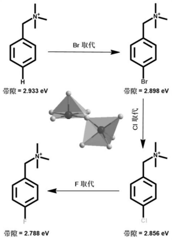
[0026] A semiconductor material having the following general structural formula:

[0027]

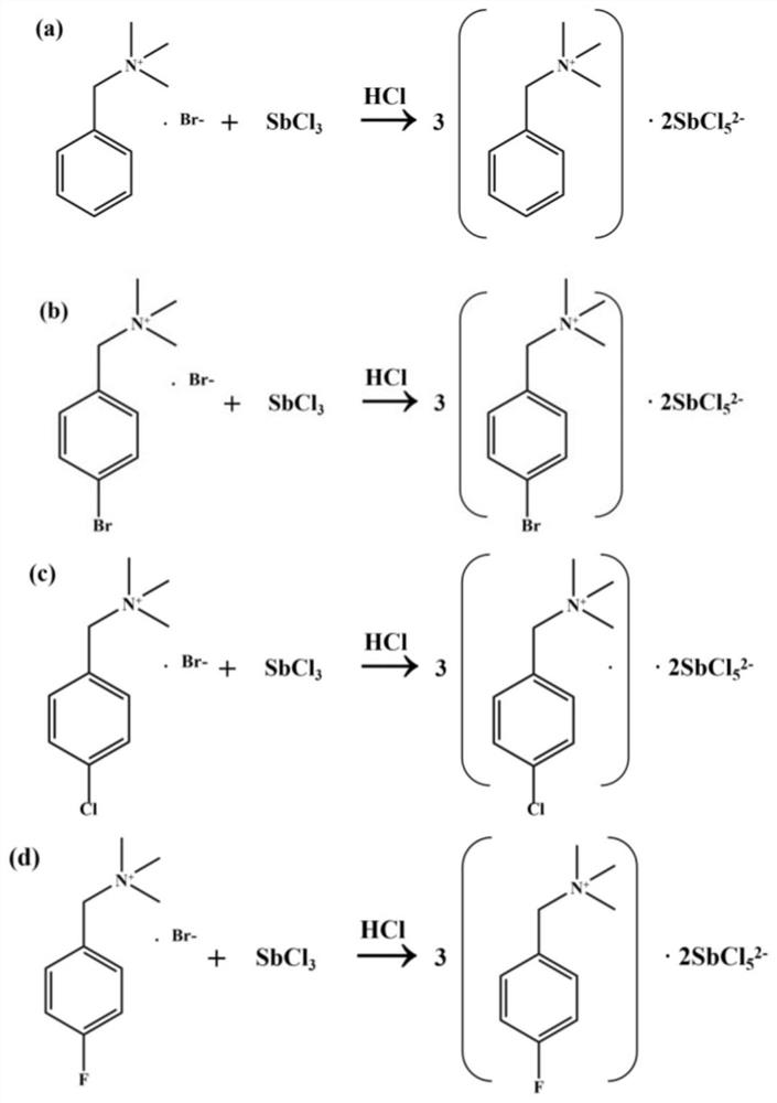
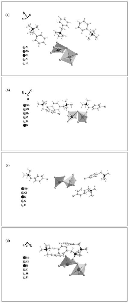
[0028] Where R=H, Br, Cl or F, the semiconductor material has a crystal structure. That is, its molecular formula is C 30 h 48 Cl 9 N 3 Sb 2 、C 30 h 45 Br 3 Cl 9 N 3 Sb 2 、C 30 h 45 Cl 12 N 3 Sb 2 and C 30 h 45 Cl 9 f 3 N 3 Sb 2 .

[0029] Its preparation method is as follows: at room temperature, 1 mol containing Sb 3+ Put the soluble compound of the beaker into a beaker and dissolve it with 33% hydrochloric acid, put 1 mol of BTAB or a derivative of BTAB (BTAB=benzyltrimethylammonium bromide) into another beaker, slowly add an appropriate amount of absolute ethanol and stir to dissolve, and then The solutions in the two beakers were then fused together, stirred at 30°C for 30 minutes, and then left to stand at room temperature for 2 weeks to obtain the semiconductor compound C 30 h 48 Cl 9 N 3 Sb 2 、C 30 h 45 Br 3 Cl 9 N 3 Sb 2 、C 30 h 45 Cl 12 ...

Embodiment 2

[0031] A semiconductor material having the following general structural formula:

[0032]

[0033] Where R=H, Br, Cl or F, the semiconductor material has a crystal structure. That is, its molecular formula is C 30 h 48 Cl 9 N 3 Sb 2 、C 30 h 45 Br 3 Cl 9 N 3 Sb 2 、C 30 h 45 Cl 12 N 3 Sb 2 and C 30 h 45 Cl 9 f 3 N 3 Sb 2 .

[0034] Its preparation method is as follows: at room temperature, 1mol containing Sb 3+ Put the soluble compound in a beaker and dissolve it with 33% hydrochloric acid, put 1.5mol of BTAB or a derivative of BTAB in another beaker, slowly add an appropriate amount of absolute ethanol and stir to dissolve, then mix the two beaker solutions with each other, at a temperature of After stirring at 35°C for 40 minutes, it was left to stand at room temperature for 2 weeks to obtain the semiconductor compound C 30 h 48 Cl 9 N 3 Sb 2 、C 30 h 45 Br 3 Cl 9 N 3 Sb 2 、C 30 h 45 Cl 12 N 3 Sb 2 、C 30 h 45 Cl 9 f 3 N 3 Sb 2 .

Embodiment 3

[0036] A semiconductor material having the following general structural formula:

[0037]

[0038] Where R=H, Br, Cl or F, the semiconductor material has a crystal structure. That is, its molecular formula is C 30 h 48 Cl 9 N 3 Sb 2 、C 30 h 45 Br 3 Cl 9 N 3 Sb 2 、C 30 h 45 Cl 12 N 3 Sb 2 and C 30 h 45 Cl 9 f 3 N 3 Sb 2 .

[0039] Its preparation method is as follows: at room temperature, 1mol containing Sb 3+ Put the soluble compound in a beaker and dissolve it with 33% hydrochloric acid, put 2 mol of BTAB or a derivative of BTAB into another beaker, slowly add an appropriate amount of acetonitrile and stir to dissolve, then mix the two beaker solutions with each other, at a temperature of 40°C After stirring for 50 minutes, it was left to stand at room temperature for about 3 weeks to obtain the semiconductor compound C 30 h 48 Cl 9 N 3 Sb 2 、C 30 h 45 Br 3 Cl 9 N 3 Sb 2 、C 30 h 45 Cl 12 N 3 Sb 2 、C 30 h 45 Cl 9 f 3 N 3 Sb 2 . ...


PUM

PropertyMeasurementUnit
band gapaaaaaaaaaa

Abstract

The invention discloses a semiconductor material and a preparation method thereof, in the structural general formula of the semiconductor material, R=H, Br, Cl or F, that is, the molecular formula of the semiconductor material is C30H48Cl9N3Sb2, C30H45Br3Cl9N3Sb2, C30H45Cl12N3Sb2 and C30H45Cl9F3N3Sb2, and the semiconductor material is of a crystal structure; the preparation method of the semiconductor material comprises the following steps: mixing a soluble compound containing Sb < 3 + > and a BTAB derivative, and carrying out self-assembly by adopting a solution natural volatilization solvent to prepare the material. The semiconductor material disclosed by the invention is relatively high in thermal decomposition temperature point and uniform in crystal particles; and meanwhile, the preparation process is simple, easy to operate, sufficient in raw material source, low in production cost, high in yield and high in repeatability.

Description

technical field [0001] The invention relates to a material and a preparation method thereof, in particular to a semiconductor material and a preparation method thereof. Background technique [0002] A semiconductor refers to a material whose conductivity at room temperature is between that of a conductor and an insulator. Refers to a material with controllable conductivity ranging from insulator to conductor. Semiconductors are used in integrated circuits, consumer electronics, communication systems, photovoltaic power generation, lighting, high-power power conversion and other fields. For example, diodes are devices made of semiconductors. No matter from the perspective of technology or economic development, the importance of semiconductors is enormous. The core units of most electronic products, such as computers, mobile phones or digital recorders, are closely related to semiconductors. Semiconductor materials often have excellent photovoltaic effects, making them impo...

Claims


Application Information

Patent Timeline
Patent Type & Authority Applications(China)
IPC IPC(8): C07C211/63C07C209/68
CPCC07C211/63C07B2200/13
Inventor 王艳宁佟亮万敏刘静苑曹龙文陈立庄
Owner JIANGSU UNIV OF SCI & TECH
Why Eureka
Try Eureka