
Boron doping method, solar cell and manufacturing method thereof

A solar cell and boron doping technology, which is applied in the manufacture of circuits, electrical components, semiconductors/solid-state devices, etc., can solve the problems of small diffusion coefficient, difficult boron doping, and high activation difficulty

Pending Publication Date: 2022-01-25
LONGI SOLAR TECH (XIAN) CO LTD
View PDF0 Cites 1 Cited by
  • Summary
  • Abstract
  • Description
  • Claims
  • Application Information

AI Technical Summary

Problems solved by technology

However, due to the small diffusion coefficient of boron in silicon materials, boron is more difficult to activate than phosphorus, which makes it difficult for boron to be doped into silicon wafers, and the doping process is more difficult.

Method used


Image

  • Boron doping method, solar cell and manufacturing method thereof
  • Boron doping method, solar cell and manufacturing method thereof
  • Boron doping method, solar cell and manufacturing method thereof

Examples


Embodiment Construction

[0039] In order to clearly describe the technical solutions of the embodiments of the present invention, in the embodiments of the present invention, words such as "first" and "second" are used to distinguish the same or similar items with basically the same function and effect. Those skilled in the art can understand that words such as "first" and "second" do not limit the number and execution order, and words such as "first" and "second" do not necessarily limit the difference.

[0040] It should be noted that, in the present invention, words such as "exemplary" or "for example" are used as examples, illustrations or illustrations. Any embodiment or design described herein as "exemplary" or "for example" should not be construed as being preferred or advantageous over other embodiments or designs. Rather, the use of words such as "exemplary" or "such as" is intended to present related concepts in a concrete manner.

[0041] In the present invention, "at least one" means one ...


PUM

PropertyMeasurementUnit
thicknessaaaaaaaaaa
wavelengthaaaaaaaaaa
particle diameteraaaaaaaaaa

Abstract

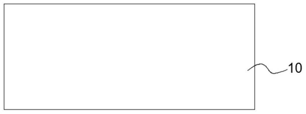
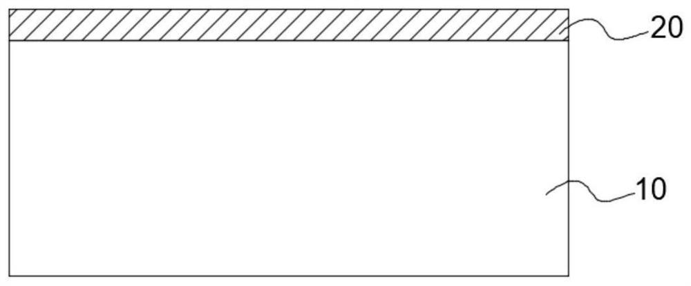
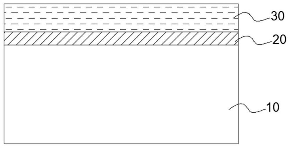
The invention discloses a boron doping method, a solar cell and a manufacturing method of the solar cell, relates to the technical field of photovoltaics, and aims to enable boron to be easily doped into a silicon wafer and reduce the boron doping difficulty. The boron doping method comprises the following steps: providing a silicon substrate; forming an auxiliary layer on the silicon substrate, wherein the material of the auxiliary layer comprises titanium dioxide; forming a boron-containing slurry layer on the auxiliary layer; propelling boron impurities in the boron-containing slurry layer through the auxiliary layer into the silicon substrate by using a laser to dope the silicon substrate. The boron doping method, the solar cell and the manufacturing method of the solar cell are used for manufacturing the solar cell.

Description

technical field [0001] The invention relates to the field of photovoltaic technology, in particular to a boron doping method, a solar cell and a manufacturing method thereof. Background technique [0002] The doping process is to dope p-type or n-type impurities into the semiconductor material, so that the doped semiconductor material has carriers. In the manufacturing process of crystalline silicon solar cells, the doping process is an important process for making pn junctions. At present, the phosphorus doping process mainly adopts the method of thermal diffusion and laser propulsion of phosphorus element in phosphosilicate glass for doping. [0003] When boron doping is performed on silicon wafers, the liquid source BBr is mainly used 3 or gaseous source BCl 3 High-temperature diffusion, etc. However, due to the small diffusion coefficient of boron in silicon materials, the activation of boron is more difficult than that of phosphorus, so boron is not easily doped int...

Claims


Application Information

Patent Timeline
Patent Type & Authority Applications(China)
IPC IPC(8): H01L21/02
CPCH01L21/02186H01L21/02321H01L21/0206
Inventor 焦云峰叶枫王建波李云朋袁陨来
Owner LONGI SOLAR TECH (XIAN) CO LTD
Learn More