Packaging structure, circuit board assembly and electronic equipment
A packaging structure and packaging cover technology, which is applied to printed circuit components, circuits, printed circuits, etc., can solve problems such as poor welding of chips and circuit boards, increased internal stress of the package, and increased power consumption of the chip, so as to improve production capacity and stability performance, reducing warpage, and reducing package weight
- Summary
- Abstract
- Description
- Claims
- Application Information
AI Technical Summary
Problems solved by technology
Method used
Image

Examples
Embodiment 1
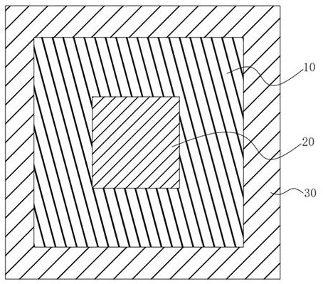
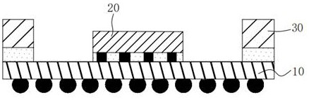
[0031] See Figure 3A , Figure 3B and Figure 3C , Figure 3A , Figure 3B and Figure 3C A structural diagram of the package structure 1 provided by one embodiment of the present invention is shown. in, Figure 3A A schematic view of a top surface structure of the package structure 1, Figure 3B for Figure 3A Schematic diagram of the profile structure in I, Figure 3C for Figure 3B Schematic diagram of the cross-sectional structure of IIII. exist Figure 3A , Figure 3B and Figure 3C In the illustrated embodiment, the package structure 1 includes a substrate 10, an electronic component 20, and a package cover 50. Wherein, the substrate 10 has a relatively disposed first surface and a second surface, the electronic component 20 connected to the first surface of the substrate 10, the package cover 50 including a top cover 510, a first support portion 521 and the second support portion 522, the top cover 510 is coupled to the first surface of the substrate 10 by the first support portion 521 ...
Embodiment 2
[0050] See Figure 4A , Figure 4b and Figure 4C , Figure 4A , Figure 4b and Figure 4C Shows a schematic structural diagram of the present invention to provide a package structure embodiment 1 of the embodiment. in, Figure 4A Is a schematic top view of the structure of package 1, Figure 4b for Figure 4A The cross-sectional structure of schematic Ⅲ, Figure 4C for Figure 4b A schematic cross-sectional structure at Ⅳ. exist Figure 4A-Figure 4C In the embodiment shown, package 1 comprises: a substrate 10, electronic components 20 and the package lid 50. Wherein, the substrate 10 having a first surface and a second surface oppositely disposed, the electronic component 20 is connected to the first surface of the substrate 10, the package lid 50 includes a top cap 510, a first support portion 521, the second supporting portion 522 and third support portions 523, 510 of the cap portion 521 by a first support, a second support portion 522 and the third supporting portion 523 is connected to ...
Embodiment 3
[0056] Please refer to Figure 5 , Figure 5 A schematic transverse cross-sectional structural diagram of a package 1 is illustrated another embodiment of the present invention. What needs to be explained, Figure 5 A top structure and a longitudinal cross-sectional structure of a package structure may correspond to the embodiment shown with reference to Figure 3A , Figure 3B The structure of the illustrated embodiment, it is omitted here. Figure 5 The package structure shown in the embodiment 1 comprises: a substrate 10, electronic components 20 and the package lid 50. Wherein, the substrate 10 having a first surface and a second surface oppositely disposed, the electronic component 20 is connected to the first surface of the substrate 10, the package lid 50 includes a top cap 510, a first support portion 521 and the second supporting portion 522, the cap 510 by the first supporting portion 521 and the second support portion 522 is connected to the first surface of the substrate 10,...
PUM
 Abstract
Description
Claims
Application Information
 - R&D Engineer
- R&D Manager
- IP Professional
- Industry Leading Data Capabilities
- Powerful AI technology
- Patent DNA Extraction
Browse by: Latest US Patents, China's latest patents, Technical Efficacy Thesaurus, Application Domain, Technology Topic.
© 2024 PatSnap. All rights reserved.Legal|Privacy policy|Modern Slavery Act Transparency Statement|Sitemap