An Adjustable High Frequency Electromagnetic Bandgap Bandpass Filter
A high-frequency electromagnetic and filter technology, which is applied in the direction of waveguide devices, circuits, electrical components, etc., can solve the problems of limited filter application, low processing precision, and large filter size, so as to improve energy storage capacity and structure Simple, the effect of improving the Q value
- Summary
- Abstract
- Description
- Claims
- Application Information
AI Technical Summary
Problems solved by technology
Method used
Image
Examples
Embodiment 1
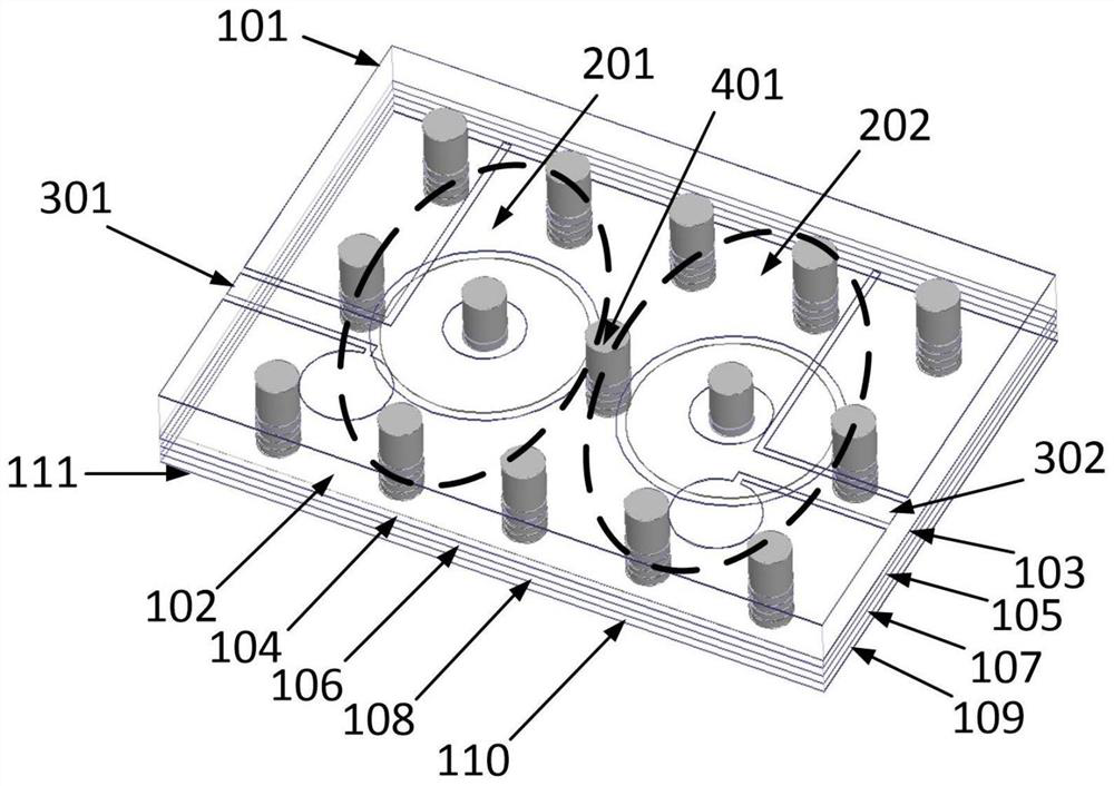
[0048] This embodiment provides an adjustable high-frequency electromagnetic bandgap bandpass filter, characterized in that the high-frequency electromagnetic bandgap bandpass filter includes: an EBG resonant cavity and a bottom stack structure;
[0049] The bottom stack structure is located at the bottom of the EBG resonant cavity, and is used to improve the energy storage capacity of the high-frequency electromagnetic bandgap bandpass filter and improve the Q value;
[0050] The EBG resonant cavity contains a capacitor structure, and the resonant frequency of the high-frequency electromagnetic bandgap bandpass filter can be adjusted by adjusting the size of the capacitor plate of the capacitor.
[0051] The high-frequency electromagnetic bandgap filter provided in this embodiment introduces a high-Q capacitor structure into the EBG cavity to greatly reduce the operating frequency of the filter, so that the small-sized EBG structure can also work in the low-frequency band, and...
Embodiment 2
[0054] This embodiment provides an adjustable high-frequency electromagnetic bandgap bandpass filter.
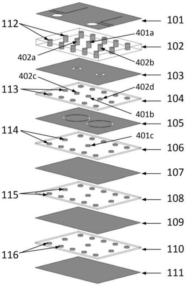
[0055] The structural decomposition of the filter of this embodiment figure 1 As shown, it includes: top layer metal plate 101, first layer dielectric plate 102, second layer through-hole metal plate 103, second layer dielectric plate 104, third layer metal plate 105, third layer dielectric plate 106, fourth layer Metal plate 107, fourth layer of dielectric plate 108, fifth layer of metal plate 109, fifth layer of dielectric plate 110 and sixth layer of bottom metal plate 111;
[0056] The top-layer metal plate 101 and the second-layer through-hole metal plate 103 are connected by a plurality of metallized through-hole arrays 401 with the same height passing through the first-layer dielectric plate 112; the second-layer through-hole metal plate 103 and the third-layer metal plate 105 are connected by a plurality of metallized via arrays 113 with the same height passing thro...
Embodiment 3
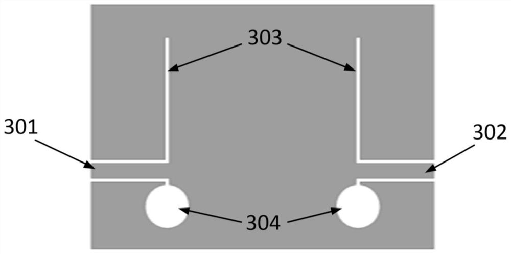
[0067] The difference between the present embodiment and the second embodiment is that, in the present embodiment, the length of the groove line 303 is 1.9mm, the radius of the metal disks 601a and 601b is 0.65mm, and the radius of the hollow circle 304 is 0.5mm. The comparison curve between the parameter simulation and the actual measurement is as follows: Figure 9 as shown in b.
PUM
| Property | Measurement | Unit |
|---|---|---|
| length | aaaaa | aaaaa |
| radius | aaaaa | aaaaa |
| length | aaaaa | aaaaa |
Abstract
Description
Claims
Application Information


