Silicon carbide joint and its metal penetration connection method

A technology of metal infiltration and connection method, which is applied in the field of ceramic material connection, can solve the problems of lower connection strength, use of solder under low temperature conditions, and accelerate the decomposition of the MAX phase of the intermediate layer, so as to achieve lower requirements, lower preparation conditions, and high-strength connection gas. tightness effect

Active Publication Date: 2022-08-02
CHINA NUCLEAR POWER TECH RES INST CO LTD +2
View PDF0 Cites 0 Cited by
  • Summary
  • Abstract
  • Description
  • Claims
  • Application Information

AI Technical Summary

Problems solved by technology

Brazing connection can be carried out under low temperature and low pressure conditions, which can meet the shape and structure requirements of silicon carbide, but most solders can only be used under low temperature conditions
[0003] The current research has found that Ti-Si brazing connection has good high temperature resistance, but this connection technology can only prepare high-strength silicon carbide joints under high vacuum conditions. When connecting in a graphite heating furnace, the MAX phase of the middle layer is accelerated. Decomposition, the connection strength is greatly reduced, which limits the application of this technology in the field of silicon carbide connection
In addition, when Ti-Si brazing connects silicon carbide, the requirements for the processing plane of silicon carbide are relatively strict, and there are requirements for the material of silicon carbide itself, which requires free carbon in the silicon carbide material, and high-purity silicon carbide is not conducive to the development of high-strength silicon carbide joints. preparation, thus limiting the application in the field of silicon carbide connections

Method used


Image

  • Silicon carbide joint and its metal penetration connection method
  • Silicon carbide joint and its metal penetration connection method
  • Silicon carbide joint and its metal penetration connection method

Examples


Embodiment 1

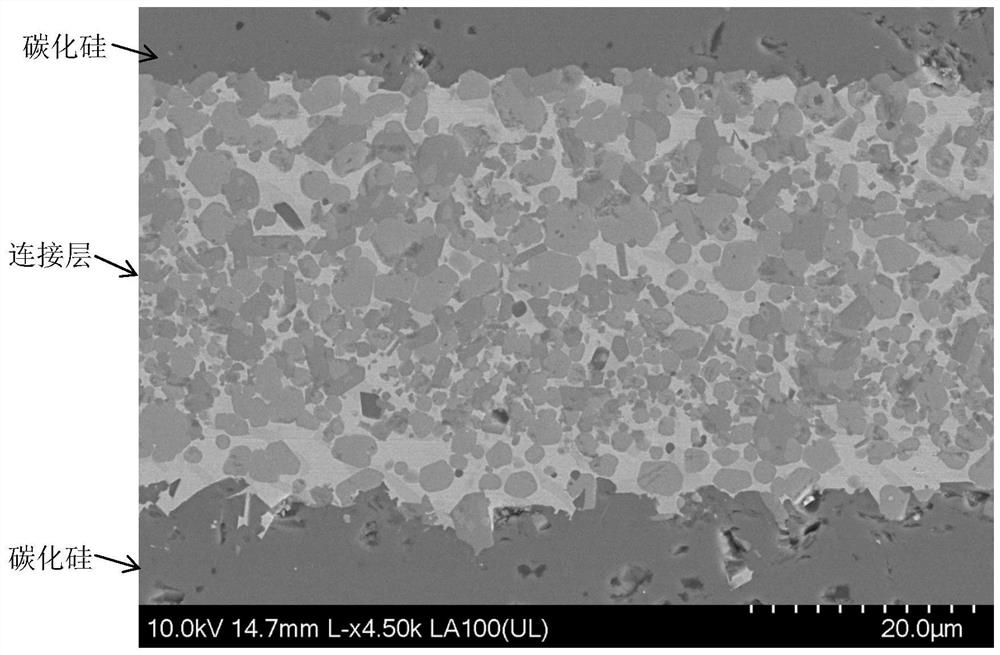
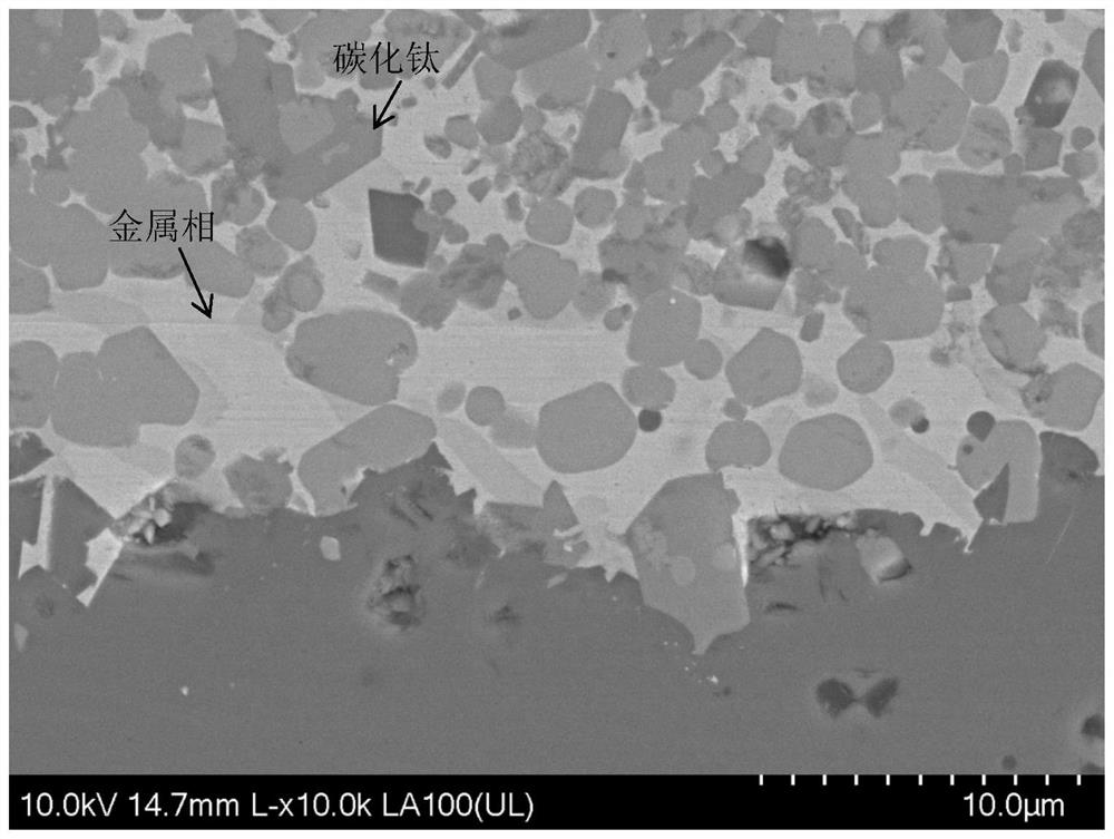
[0053]Metal Ti foil (thickness 10 μm, purity 99.99%) and Si powder (particle size 1 μm, purity 99.999%) are used as the raw materials of the connecting material; after the metal Ti foil is polished with sandpaper, the Si powder is smeared on both sides of the metal Ti foil. On the other hand, the molar ratio of metal Ti foil and Si powder is 2:3; the above metal Ti foil and Si powder are placed between silicon carbide to form a sandwich structure. In a graphite crucible, the above sandwich structure is placed around the iron, cobalt, and nickel blocks, and then the graphite crucible is placed in a sintering furnace for sintering connection. During sintering, the temperature was raised to 1500° C. at 20° C. / min, and the temperature was maintained for 1 h. The sintering atmosphere was vacuum, and a silicon carbide joint was obtained after sintering.

[0054] The SEM image of the silicon carbide joint obtained above is as follows figure 1 shown. from figure 1 It can be seen th...

Embodiment 2

[0057] Metal Mo (thickness 20 μm, purity 99.99%) and Si powder (particle size 5 μm, purity 99.999%) were used as the raw materials of the connecting material; the connection of silicon carbide was realized according to the method of Example 1, wherein during sintering, the sintering temperature was 1600 ℃, holding the temperature for 2h, and the sintering atmosphere is argon, to obtain a silicon carbide joint with a dense connection layer.

[0058] For the silicon carbide joint prepared above, the thickness of the connecting layer is 60 μm. In the shear strength test, the shear strength at room temperature is 120MPa, and the shear strength at a high temperature of 1200°C is 150MPa. Silicon carbide joints have a leak rate of 1×10 -9 Pa·L / s.

Embodiment 3

[0060] Metal Ta (thickness 20 μm, purity 99.99%) and Al powder (particle size 20 μm, purity 99.999%) were used as the raw materials of the connection material; the connection of silicon carbide was realized according to the method of Example 1, wherein during sintering, the sintering temperature was 1700 ℃, holding the temperature for 2h, and the sintering atmosphere is argon, to obtain a silicon carbide joint with a dense connection layer.

[0061] For the silicon carbide joint prepared above, the thickness of the connecting layer is 50 μm. In the shear strength test, the shear strength at room temperature is 150MPa, and the shear strength at a high temperature of 1200°C is 200MPa. Silicon carbide joints have a leak rate of 1×10 -8 Pa·L / s.


PUM

PropertyMeasurementUnit
thicknessaaaaaaaaaa
shear strengthaaaaaaaaaa

Abstract

The invention discloses a silicon carbide joint and a metal penetration connection method thereof. The metal penetration connection method includes the following steps: S1, preparing a first metal raw material and a second metal raw material to form a connecting material; S2, disposing the connecting material in a Between the connection surfaces of the two silicon carbide pieces, a sandwich structure is formed with the two silicon carbide pieces; S3, the sandwich structure is placed in a sintering environment with a metal phase and sintered; during the sintering process, the metal phase infiltrates into the connecting material and fill in the pores generated in the connecting material; S4, after sintering, the connecting material is densified to form a connecting layer, and two silicon carbide parts are connected to form a silicon carbide joint. The metal infiltration connection method of the silicon carbide joint of the present invention penetrates into the connecting material with the metal phase, realizes the densification of the connecting material, obtains a high-strength connection and a silicon carbide joint with good air tightness, and reduces the requirements on the shape and structure of silicon carbide. .

Description

technical field [0001] The invention relates to the technical field of ceramic material connection, in particular to a silicon carbide joint and a metal penetration connection method thereof. Background technique [0002] Silicon carbide ceramics have high melting point, excellent mechanical, thermal and corrosion resistance properties, making them widely used in vehicles, marine engineering, nuclear energy, aerospace and other fields. The above applications not only require silicon carbide to have good high temperature resistance, but also have high requirements for its shape and structure. The brazing connection can be carried out under low temperature and low pressure conditions, which can meet the requirements of the shape and structure of silicon carbide, but most of the brazing materials can only be used under low temperature conditions. [0003] Current research has found that Ti-Si brazing joints have good high temperature resistance, but this joint technology can o...

Claims


Application Information

Patent Timeline
Patent Type & Authority Patents(China)
IPC IPC(8): C04B37/00
CPCC04B37/003C04B2237/12C04B2237/121C04B2237/365
Inventor 吴利翔薛佳祥廖业宏任啟森翟剑晗张永栋张显生
Owner CHINA NUCLEAR POWER TECH RES INST CO LTD
Why Eureka
Try Eureka