Bidirectional silicon-controlled rectifier

A silicon controlled rectifier, N-type technology, applied in the direction of semiconductor devices, electric solid state devices, electrical components, etc., to achieve the effects of low parasitic capacitance, optimized device performance, and low trigger voltage

Pending Publication Date: 2022-02-18
SHANGHAI CHANGYUAN WAYON MICROELECTRONICS
View PDF0 Cites 0 Cited by
  • Summary
  • Abstract
  • Description
  • Claims
  • Application Information

AI Technical Summary

Problems solved by technology

like figure 1 In the traditional structure shown, the parasitic capacitance of the device is mainly formed by the two junctions of NW / PW and NW / P substrate. Usually, a thicker NW process is used to achieve a low trigger voltage, which will inevitably lead to a larger parasitic capacitance.

Method used


Image

  • Bidirectional silicon-controlled rectifier
  • Bidirectional silicon-controlled rectifier
  • Bidirectional silicon-controlled rectifier

Examples


Embodiment 1

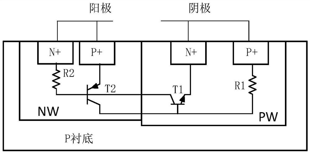
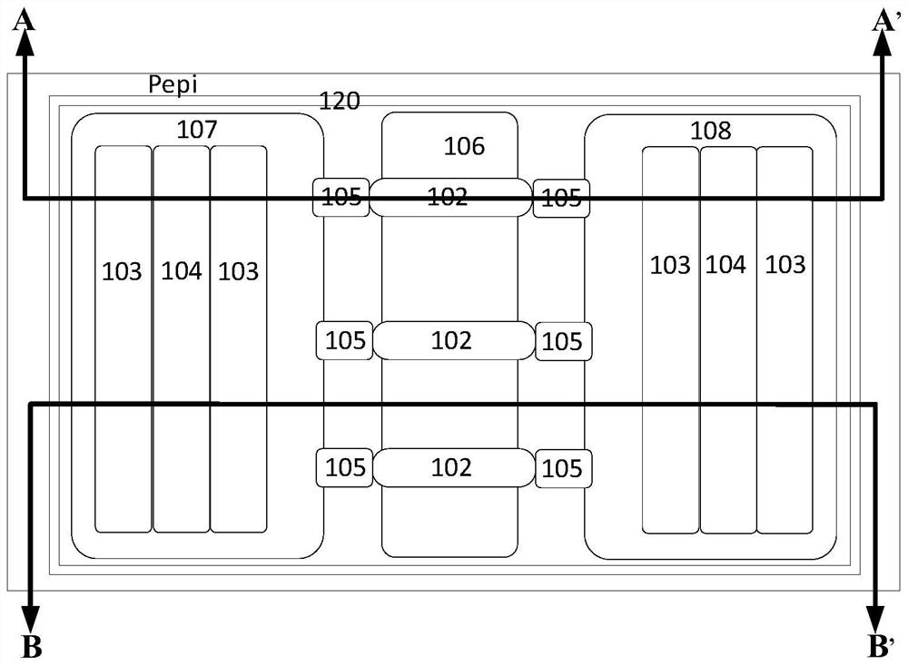
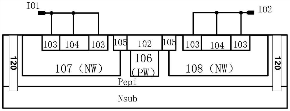
[0048] Such as Figure 2 ~ Figure 4 , the bidirectional silicon-controlled rectifier proposed in the present invention includes a substrate epitaxial crystal, specifically, the substrate epitaxial crystal is an N-type conductive substrate and a P-type conductive epitaxy; it also includes a silicon-controlled rectifier region formed in the substrate epitaxial crystal, The silicon controlled rectifier region includes a first N-type well region 107 , a second N-type well region 108 , and a first P-type well region 106 . The first P-type well region 106 is located between the first N-type well region 107 and the second N-type well region 108; the first N-type well region 107 includes an N-type heavily doped region 103 and a P-type heavily doped region 104 , the N-type heavily doped region 103 and the P-type heavily doped region 104 are connected through metal and connected to the input port IO1; the second N-type well region 108 includes the N-type heavily doped region 103 and the...

Embodiment 2

[0055] Such as Figure 5 As shown, the difference from Implementation Example 1 is that the trigger region process is different. The N-type doped region 105 is no longer located on the surface, but symmetrically located under the P-type doped region 102. This solution can be realized by using a larger implant energy . The advantage is that the internal area is fully utilized, the surface area of ​​the device is reduced, and the influence of overlay deviation can be avoided in small-scale processes. The N-type doped region 105 partially overlaps the N-type well region 107 , but the N-type doped region 105 in the N-type well region 107 and the N-type well region 108 cannot connect across the P-type well region 106 . In the second implementation example, the trigger voltage of the bidirectional silicon controlled rectifier is still controlled by the diode formed by the N-type doped region 105 and the P-type doped region 102 in the trigger region. Preferably, the P-type doped reg...

Embodiment 3

[0057] Such as Figure 6 As shown, the difference from Implementation Example 1 is that it is fabricated on a P-type substrate and an N-type epitaxial crystal, and the corresponding silicon-controlled rectifier area and trigger area are changed:

[0058] The silicon controlled rectifier region includes a first P-type well region 109 , a second P-type well region 110 , and a first N-type well region 111 . The first N-type well region 111 is located between the first P-type well region 109 and the second P-type well region 110; the first P-type well region 109 includes an N-type heavily doped region 103 and a P-type heavily doped region 104 , the N-type heavily doped region 103 and the P-type heavily doped region 104 are connected through metal and connected to the input port IO1; the second P-type well region 110 includes the N-type heavily doped region 103 and the P-type heavily doped region 104, the N-type heavily doped region 103 and the P-type heavily doped region 104 are ...


PUM


Abstract

A bidirectional silicon-controlled rectifier is provided by the invention, and comprises a substrate epitaxial crystal, a silicon-controlled rectifier region and a trigger region, the silicon-controlled rectifier region and the trigger region are located on the substrate epitaxial crystal, one end of the silicon-controlled rectifier is connected to an input end IO1 through metal, the other end of the silicon-controlled rectifier is connected to an output end IO2 through metal, and ESD protection and EOS protection in the IO1-IO2 direction and the IO2-IO1 direction are formed. According to the bidirectional silicon-controlled rectifier, the floating complementary doped region and the transfer avalanche breakdown point are added on the structure of the traditional bidirectional silicon-controlled rectifier, and the floating trigger region is designed to be the minimum size, so that low trigger voltage and low parasitic capacitance are realized at the same time.

Description

technical field [0001] The invention relates to a semiconductor device, in particular to a bidirectional silicon-controlled rectifier. Background technique [0002] In recent years, the rapid development of integrated circuit manufacturing technology has brought rapid upgrading of electronic products. In order to ensure the quality and reliability of electronic products, the chips and external interface circuits must have a certain level of anti-ESD (Electro-Static discharge, static electricity Discharge) capability, so more and more protective devices are required. Thyristor, as a protection device with strong robustness per unit area and small parasitic capacitance, is widely used in various products. Traditional SCR (Silicon Controlled Rectifier, Silicon Controlled Rectifier) ​​structure such as figure 1 As shown, two back-to-back triodes are connected in series to form a P+ / NW / PW / N+ path between the anode and the cathode. When the pulse current from the anode to the ca...

Claims


Application Information

Patent Timeline
Patent Type & Authority Applications(China)
IPC IPC(8): H01L27/02
CPCH01L27/0262H01L27/0292
Inventor 吴昊陆亚斌
Owner SHANGHAI CHANGYUAN WAYON MICROELECTRONICS
Why Eureka
Try Eureka