
Eureka
For R&D, Eureka makes reading and utilizing patents & technical documents easy.
Eureka AIR
Designed for self-driven R&D workflows. Generate viable solutions, solve complex R&D challenges, empower your innovation with AI.

Eureka Materials
Designed for material experts only. Revolutionize your material R&D, from search, analyze, to developing new materials.

TechResearch
Generate reliable direction feasibility study reports for your R&D in just a few steps.

TechSeek
Discover and master advanced knowledge NOW. Basics, ideas, possibilities, all at once.

TechMind
As an expert in R&D Theories, TechMind can generates customized viable solutions instantly.

TechRisk
Analyze your overall solution with one click, know your potential R&D risks in advance.

TechMonitor
Get weekly tech updates, stay abreast of the latest tech innovations and key insights.
Dual-surface acoustic wave filter, dual-frequency assembly and manufacturing method of dual-surface acoustic wave filter
A surface acoustic wave and filter technology, applied to electrical components, impedance networks, etc., can solve the problems of high processing cost, poor reliability at the junction, and signal loss, etc., and achieve low design difficulty, optimal device performance, and simple manufacturing process Effect
- Summary
- Abstract
- Description
- Claims
- Application Information
AI Technical Summary
Problems solved by technology
Method used
Image

Examples
Embodiment 1
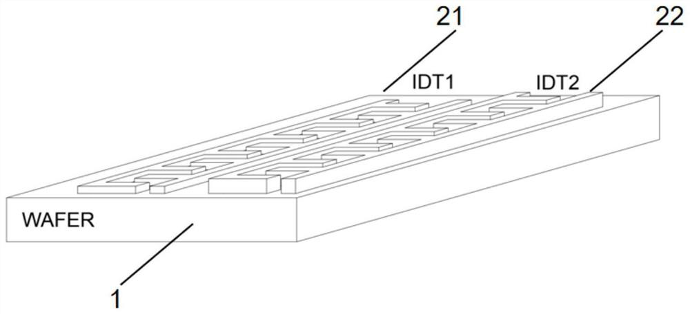
[0051] A specific embodiment of the present invention, such as figure 2 As shown, a structural schematic diagram of a double surface acoustic wave filter is disclosed, and the double surface acoustic wave filter includes:
[0052] A piezoelectric substrate 1, on which a first filter element and a second filter element are arranged. The first filter element responds to the first frequency of the surface acoustic wave, the first filter element includes a plurality of first IDT electrode fingers 21, the first IDT electrode fingers 21 have a first metal film with a first thickness, and a plurality of first IDT electrodes The fingers 21 are mounted on the piezoelectric substrate along the propagation direction of the surface acoustic wave.
[0053] Further, the second filter element responds to the second frequency of the acoustic surface, the second filter element includes a plurality of second IDT electrode fingers 22, the second IDT electrode fingers have a second metal film w...
Embodiment 2
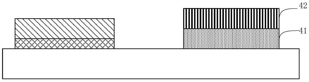
[0070] A specific embodiment of the present invention also discloses a structural schematic diagram of a double surface acoustic wave filter, as Figure 10 As shown, the dual surface acoustic wave filter includes:
[0071] The first IDT electrode fingers 21 are formed on the upper surface of the piezoelectric single crystal substrate, and the second IDT electrode fingers 22 are formed on the lower surface of the piezoelectric single crystal substrate. The entire IDT electrode fingers are arranged in concavo-convex manner on the piezoelectric single crystal substrate. The depth of the concavo-convex structure is less than or equal to the depth of the piezoelectric single crystal substrate. Specifically, the arrangement of the concave-convex structure corresponding to the surface IDT electrodes is implemented to be or alternately arranged with the IDT electrodes, or every two concave-convex structures correspond to the width of one IDT electrode finger, thereby reducing inserti...
Embodiment 3
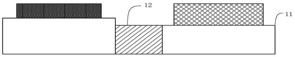
[0074] A specific embodiment of the present invention, such as Figure 11 As shown, a structural schematic diagram of another double surface acoustic wave filter is disclosed. The double surface acoustic wave filter includes a piezoelectric substrate, and the piezoelectric substrate includes:
[0075] The piezoelectric single crystal film 31, the first filter element and the second filter element are located on the same surface of the piezoelectric single crystal film.
[0076] The bonding layer 32 is disposed on the surface of the piezoelectric single crystal thin film away from the first filter element. The bonding layer has a positive temperature compensation coefficient TCF, and can be realized as silicon dioxide, for example. The supporting substrate 33 is disposed on the surface of the bonding layer 32 away from the piezoelectric single crystal thin film, and the supporting substrate is a single crystal silicon substrate. Thus, the dual surface acoustic wave filter can ...
PUM
 Abstract
Description
Claims
Application Information
 - R&D Engineer
- R&D Manager
- IP Professional
- Industry Leading Data Capabilities
- Powerful AI technology
- Patent DNA Extraction
Browse by: Latest US Patents, China's latest patents, Technical Efficacy Thesaurus, Application Domain, Technology Topic, Popular Technical Reports.
© 2024 PatSnap. All rights reserved.Legal|Privacy policy|Modern Slavery Act Transparency Statement|Sitemap|About US| Contact US: help@patsnap.com