Supercharge Your Innovation With Domain-Expert AI Agents!

Interface circuit, data transmission circuit and memory

A technology of data transmission circuit and interface circuit, which is applied in the field of data transmission circuit, memory and interface circuit, can solve the problems of DRAM performance to be improved, and achieve the effects of superior structural performance, improved matching degree, and reduced clock path

Pending Publication Date: 2022-03-01
CHANGXIN MEMORY TECH (SHANGHAI) INC
View PDF0 Cites 1 Cited by
  • Summary
  • Abstract
  • Description
  • Claims
  • Application Information

AI Technical Summary

Problems solved by technology

[0004] However, current DRAM performance still needs to be improved

Method used


Image

  • Interface circuit, data transmission circuit and memory
  • Interface circuit, data transmission circuit and memory
  • Interface circuit, data transmission circuit and memory

Examples


Embodiment Construction

[0038] It can be seen from the background art that the performance of the DRAM in the prior art still needs to be improved.

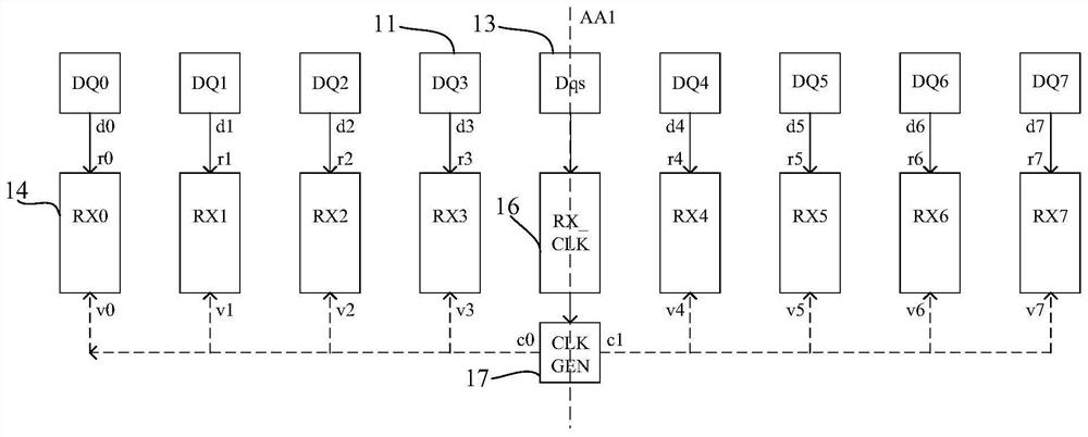
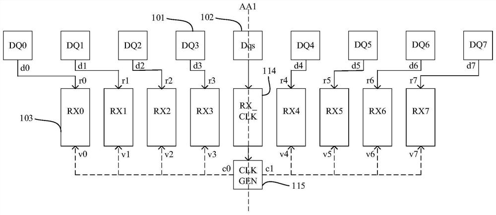
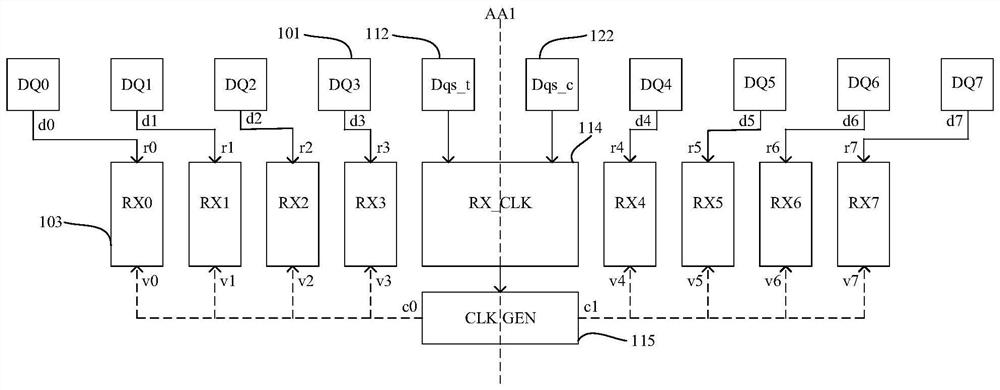
[0039]In the memory, the write data sampling signal (Dqs signal or Wck signal) is used as the clock for writing data; during the write operation, the edge (rising edge and falling edge) of the Dqs or Wck signal should be in timing with the data signal (DQ signal ) (substantially aligned at the center may also be allowed for timing margins). The transmission path of the DQ signal is defined as the data path, and the length of the data path will affect the time when the edge of the DQ signal reaches the device port (such as the data port of the register). The transmission path of the Dqs or Wck signal is defined as the clock path, and the length of the clock path will affect Affects when the Dqs or Wck signal arrives at a device port (such as the clock port of a register), and the difference between the data path of the DQ signal and the clock path of the...


PUM


Abstract

The embodiment of the invention provides an interface circuit, a data transmission circuit and a memory, the interface circuit comprises a clock bonding pad, data bonding pads and an input buffer circuit, the clock bonding pad and the data bonding pads are arranged in a first row, M data bonding pads are arranged on two sides of the clock bonding pad, half of the M data bonding pads are arranged on each side, the M input buffer circuits are arranged in the second row, an axis perpendicular to the first row is formed by taking the data bonding pad as a reference, the M input buffer circuits are arranged on the two sides of the axis, half of the M input buffer circuits are arranged on each side, and the distance between each input buffer circuit and the axis is smaller than the distance between the data bonding pad corresponding to the input buffer circuit and the axis. According to the embodiment of the invention, the length of the clock path corresponding to each input buffer circuit is shortened, the time sequence violation is reduced, and the matching degree of the clock path corresponding to each input buffer circuit and the input data path is improved.

Description

technical field [0001] The embodiments of the present invention relate to the technical field of semiconductors, and in particular to an interface circuit, a data transmission circuit and a memory. Background technique [0002] Dynamic Random Access Memory (Dynamic Random Access Memory, DRAM) is a semiconductor storage device commonly used in computers, and is composed of many repeated storage units. Each memory cell usually includes a capacitor and a transistor. The gate of the transistor is connected to the word line, the drain is connected to the bit line, and the source is connected to the capacitor. The voltage signal on the word line can control the opening or closing of the transistor, and then through the bit line Read the data information stored in the capacitor, or write the data information into the capacitor through the bit line for storage. [0003] DRAM can be divided into Double Data Rate (DDR) DRAM, GDDR (Graphics Double Data Rate) DRAM, and Low Power Double...

Claims


Application Information

Patent Timeline
IPC IPC(8): G11C11/4093H03M9/00
CPCG11C11/4093H03M9/00G11C7/1084G11C7/1093G11C7/222G11C5/063G11C11/4076G11C2207/105G11C7/1057G11C7/1066G11C5/025G11C11/4096
Inventor 林峰
Owner CHANGXIN MEMORY TECH (SHANGHAI) INC
Features
  • R&D
  • Intellectual Property
  • Life Sciences
  • Materials
  • Tech Scout
  • Unparalleled Data Quality
  • Higher Quality Content
  • 60% Fewer Hallucinations
Learn More