Wafer lifting column, preparation method thereof and wafer processing equipment

A technology for processing equipment and lifting columns, applied in semiconductor/solid-state device manufacturing, electrical components, circuits, etc., can solve problems such as film thickness uniformity, plasma field distribution, and debris, so as to ensure yield and production capacity, Reduce the probability of breaking and reduce the effect of PA

Pending Publication Date: 2022-03-04
PIOTECH CO LTD
View PDF1 Cites 0 Cited by
  • Summary
  • Abstract
  • Description
  • Claims
  • Application Information

AI Technical Summary

Problems solved by technology

However, the upper part of this patent is a ceramic structure, which is easy to break, which may easily cause wafer position deviation, process abnormalities, and even fragments, which will affect the production capacity of the machine; and the ceramic structure also has low electrostatic conductivity. The problem is that it is easy to generate discharge phenomenon on the back of the wafer, which affects the distribution of the plasma field, which will affect the uniformity of the film thickness.
Moreover, in order to realize the height adjustment of the upper part of this patent, one end of the upper part has an inner hole, and the upper part is a ceramic structure, which is easier to break

Method used


Image

  • Wafer lifting column, preparation method thereof and wafer processing equipment
  • Wafer lifting column, preparation method thereof and wafer processing equipment
  • Wafer lifting column, preparation method thereof and wafer processing equipment

Examples


Embodiment Construction

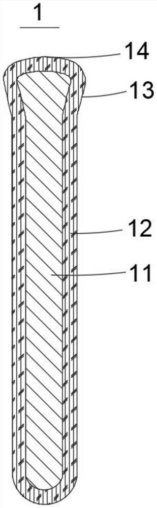
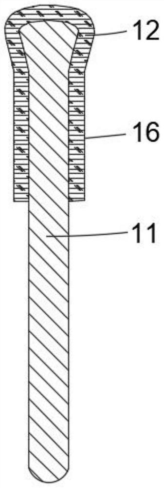
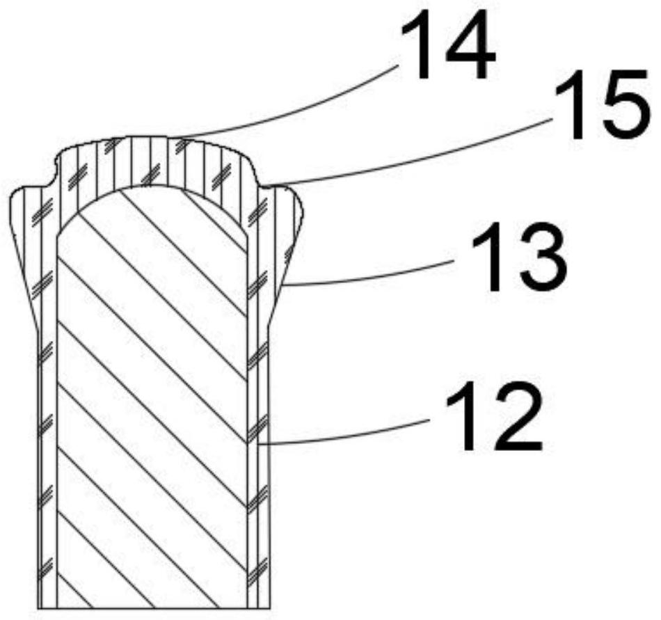
[0032] In order to make the purpose, technical solutions and advantages of the embodiments of the present invention clearer, the technical solutions in the embodiments of the present invention will be clearly and completely described below. Obviously, the described embodiments are part of the embodiments of the present invention, not all of them. the embodiment. Based on the embodiments of the present invention, all other embodiments obtained by persons of ordinary skill in the art without creative efforts fall within the protection scope of the present invention. Unless otherwise defined, the technical terms or scientific terms used herein shall have the usual meanings understood by those skilled in the art to which the present invention belongs. As used herein, "comprising" and similar words mean that the elements or items appearing before the word include the elements or items listed after the word and their equivalents, without excluding other elements or items.

[0033] ...


PUM

PropertyMeasurementUnit
thicknessaaaaaaaaaa
lengthaaaaaaaaaa
thicknessaaaaaaaaaa

Abstract

The invention provides a wafer lifting column which is arranged in a semiconductor base and used for lifting a wafer, the wafer lifting column comprises a metal base body and a ceramic coating, and the ceramic coating is arranged on the outer surface of the metal base body, so that the probability of breakage of the wafer lifting column is reduced, generation of PA is reduced, and the yield of the wafer lifting column is improved. Namely, the metal matrix made of the metal material is good in conductivity and can effectively transfer static electricity, the metal matrix is easy to process, high in formability, good in toughness and not prone to being broken, the ceramic coating is resistant to abrasion, the problem caused by PA standard exceeding can be solved, the ceramic coating can be repeatedly processed, and the service life of the ceramic coating is prolonged. And a bearing structure for bearing the wafer at the top of the wafer lifting column can be renovated for use. The invention also provides a preparation method of the wafer lifting column and wafer processing equipment.

Description

technical field [0001] The invention relates to the technical field of semiconductor manufacturing, in particular to a wafer lifting column, a preparation method thereof, and wafer processing equipment. Background technique [0002] In the existing semiconductor coating equipment, especially in the 12-inch semiconductor coating equipment, various forms of pins (Pins) for supporting and lifting the wafer need to be applied. For example, in the film forming process, in order to transfer the wafer between the vacuum robot and the heating plate, the wafer needs to be lifted and lowered smoothly on the heating plate, and the smooth lifting of the wafer needs to be lifted and lowered in the lifting hole of the heating plate through the Pin And the drive is done. [0003] The Chinese patent with publication number CN213093186U discloses a thimble, a lifting mechanism and a semiconductor machine. The thimble includes an upper part and a lower part, one end of the upper part is scr...

Claims


Application Information

Patent Timeline
Patent Type & Authority Applications(China)
IPC IPC(8): H01L21/687H01L21/67
CPCH01L21/68742H01L21/68757H01L21/67011
Inventor 谈太德郭月杨辰烨陈新益
Owner PIOTECH CO LTD
Why Eureka
Try Eureka