Defect detection method, mask manufacturing method and semiconductor structure forming method

A defect detection and defect technology, which is applied in semiconductor/solid-state device testing/measurement, photolithographic process of patterned surface, optics, etc., can solve the problem that the yield rate of semiconductor structure needs to be improved, and achieve the effect of improving yield rate

Pending Publication Date: 2022-03-11
SEMICON MFG INT (SHANGHAI) CORP +1
View PDF0 Cites 0 Cited by
  • Summary
  • Abstract
  • Description
  • Claims
  • Application Information

AI Technical Summary

Problems solved by technology

[0004] However, the yield rate of the semiconductor structure formed by the optical proximity corrected mask in the prior art still needs to be improved

Method used


Image

  • Defect detection method, mask manufacturing method and semiconductor structure forming method
  • Defect detection method, mask manufacturing method and semiconductor structure forming method
  • Defect detection method, mask manufacturing method and semiconductor structure forming method

Examples


Embodiment Construction

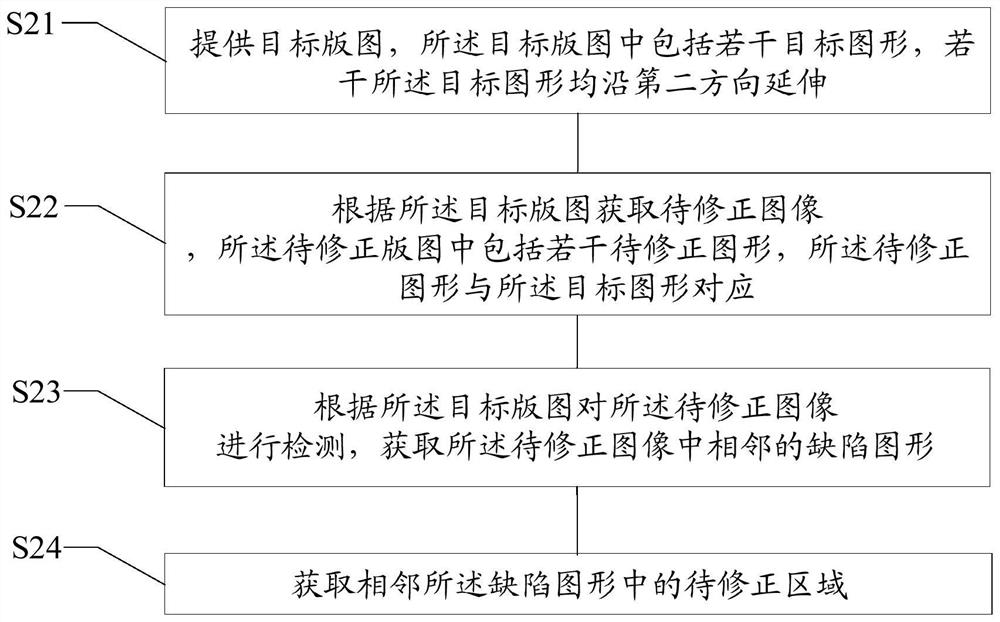
[0039] As mentioned in the background, the yield of the semiconductor structure formed by the optical proximity corrected mask in the prior art still needs to be improved. The following will describe in detail in conjunction with the accompanying drawings.

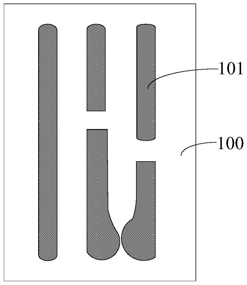
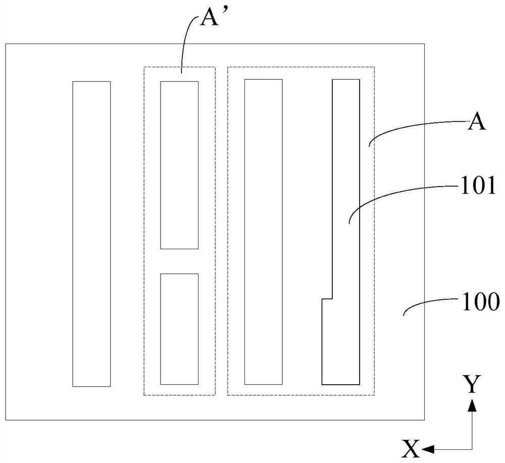
[0040] Please refer to figure 1 , providing a substrate 100, the surface of the substrate has a layer to be etched (not shown); providing a mask (not shown); using the mask as a mask, the layer to be etched is patterned process, forming several core layers 101 on the substrate.

[0041] In this embodiment, although the reticle has undergone several optical proximity corrections, as the current minimum feature size continues to decrease, the graphics in the reticle will be short-circuited during the exposure process ( bridge), if this short circuit phenomenon is solved only by its own mask, in some cases it will be very cumbersome and difficult, or even impossible to solve, so it will cause a short circuit between the fin...


PUM


Abstract

The invention discloses a defect detection method, a mask manufacturing method and a semiconductor structure forming method, and the method comprises the steps: providing a target layout which comprises a plurality of target patterns, and the plurality of target patterns extend in a second direction; obtaining a to-be-corrected image according to the target layout, the to-be-corrected image comprising a plurality of to-be-corrected graphs, and the to-be-corrected graphs corresponding to the target graph; detecting the to-be-corrected image according to the target layout, and obtaining adjacent defect patterns in the to-be-corrected image; and obtaining a to-be-corrected area in the adjacent defect pattern. Through the obtained to-be-corrected area, a correction basis is provided for subsequent correction of the formation of a mask and a semiconductor structure.

Description

technical field [0001] The invention relates to the technical field of semiconductor manufacturing, in particular to a defect detection method, a mask plate manufacturing method and a semiconductor structure forming method. Background technique [0002] Photolithography technology is a crucial technology in semiconductor manufacturing technology. Photolithography technology can realize the transfer of graphics from the mask to the surface of the silicon wafer to form semiconductor products that meet the design requirements. However, the existing photolithography technology is often accompanied by the optical proximity effect. [0003] In order to correct the optical proximity effect, an optical proximity correction (OPC: Optical ProximityCorrection) is produced. The core idea of ​​optical proximity correction is to establish the optical proximity correction model based on the consideration of offsetting the optical proximity effect, and design the photomask pattern accordin...

Claims


Application Information

Patent Timeline
Patent Type & Authority Applications(China)
IPC IPC(8): G03F1/36G03F1/72G03F1/84H01L21/66
CPCG03F1/72G03F1/84G03F1/36H01L22/12H01L22/20
Inventor 高亚新沈泫李忠生游亚平
Owner SEMICON MFG INT (SHANGHAI) CORP
Why Eureka
Try Eureka