
MEMS packaging method

A method of encapsulation and a technology for encapsulating shells, which are applied in the fields of decorative arts, microstructure devices, and manufacturing microstructure devices, etc., which can solve problems such as rising product costs, small expenses for depreciated finished products, and impact on product competitiveness, and achieve low plastic packaging costs , Saving packaging costs, the effect of unaffected competitiveness

Pending Publication Date: 2022-03-18
SUZHOU GOODARK ELECTRONICS CO LTD
View PDF0 Cites 0 Cited by
  • Summary
  • Abstract
  • Description
  • Claims
  • Application Information

AI Technical Summary

Problems solved by technology

Although the vacuum coating technology is very mature, there are the following defects in this type of products. One is that the coating resin has a certain thickness, usually up to 0.15mm, which increases the thickness of the product by 0.15mm; moreover, the coating resin is expensive , currently imported materials, the price of a piece of 90*90mm resin exceeds 100 yuan, which increases the cost of a single product by nearly 0.1 yuan; in addition, the lamination process also requires the addition of expensive lamination equipment, a single machine reaches 200,000 US dollars, and the finished product is depreciated The product is also not a small expense
[0006] The above results in an increase in product thickness, which limits the application of ultra-thin products required by the client and affects market promotion; the increase in product costs also affects the competitiveness of the product

Method used


Image

  • MEMS packaging method
  • MEMS packaging method
  • MEMS packaging method

Examples


Embodiment

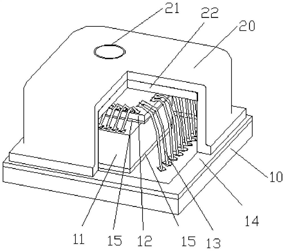
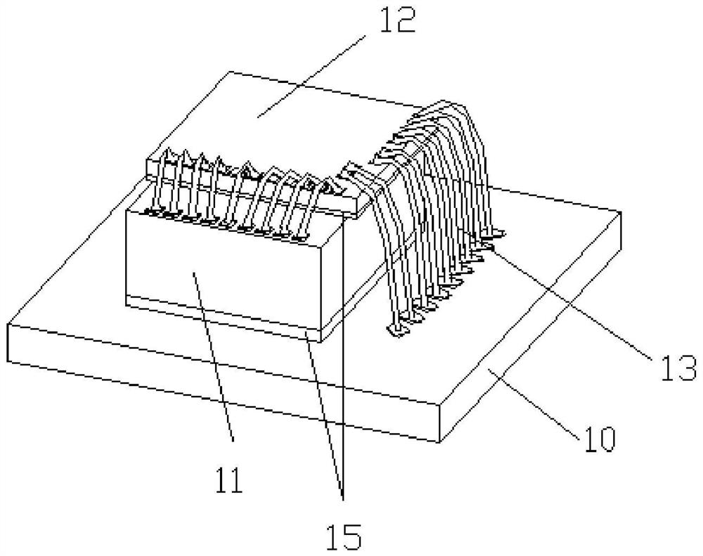
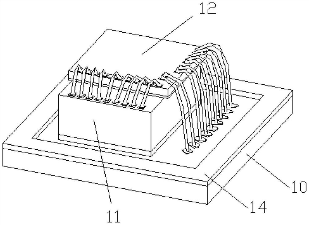
[0047] Example: Figure 1-5 As shown, a MEMS packaging method includes the following steps:

[0048] Step 1: Assembly: figure 2 As shown, the chip group is attached to the substrate 10, and the gold wire 13 is connected to the chipset and the substrate 10 after baked.

[0049] Step 2: Painting the solder paste and cap: Apply the solder paste 14 points on the copper foil around the substrate, such as image 3 Disted, will Figure 4 The encapsulation housing 20 is provided on the solder paste 14 of the substrate, and the solder paste is soldered by reflow, and the package housing 20 is welded to the substrate 10, and the semi-finished product is obtained, wherein the top surface of the package housing is provided. Small hole 21;

[0050] Step 3: Invert the clipping hole: The upper surface of the top surface of the package housing is bonded to the flip mold of the epoxy resin. After heating, the epoxy resin is placed into the cavity of the package housing through the small hole 21 and blo...


PUM


Abstract

The invention relates to an MEMS (Micro Electro Mechanical System) packaging method, which comprises the following steps of: mounting a chip group on a substrate, baking, and connecting a gold wire between the chip group and the substrate in a bonding manner; solder paste is dispensed on the copper foil on the periphery of the substrate, the packaging shell covers the solder paste on the substrate, and the solder paste is melted through reflow soldering, so that the packaging shell is welded with the substrate; the upper surface of the top face of the packaging shell is attached to an inverted mold with epoxy resin, and after heating, the epoxy resin is squeezed into the cavity of the packaging shell through the small hole and blocks the small hole; curing the product, so that the epoxy resin in the cavity and the small hole of the packaging shell is cured; laser lettering is conducted on the product according to requirements; and cutting the product into single finished products by using a cutting machine. According to the method, the purpose of plugging the small holes is achieved, meanwhile, the size of a product is not increased, the production cost of the product is not increased, and the practicability is very high.

Description

Technical field [0001] The present invention relates to a packaging method, and more particularly to a low cost MEMS package method. Background technique [0002] With the in-depth development of MEMS, MEMS's application is increasing, and the requirements for MEMS are also increasing, such as noise requirements, drift, etc. for MEMS, with the development of electronic products, for the use of MEMS devices Accuracy and so on put forward higher requirements. [0003] The detection of MEMS is achieved by micromechanical movement, and the mechanical stress affecting micromechanical has always been one of the main factors that plague MEMS performance improvement. The stress source is mainly due to different materials that are in contact with each other after the MEMS package, such as The plastic resin wrapped in the MEMS chip, the welding reflux after the cover, especially after the development of multi-chip assembled SIP, used in thin and small electronic products, the shape require...

Claims


Application Information

Patent Timeline
IPC IPC(8): B81C1/00B81B7/02
CPCB81C1/00261B81C1/00269B81B7/02
Inventor 郑志荣吴炆皜陈学峰胡乃仁
Owner SUZHOU GOODARK ELECTRONICS CO LTD
Learn More