Supercharge Your Innovation With Domain-Expert AI Agents!

Vertically stacked complementary field effect transistor and preparation method thereof

A technology of field effect transistors and vertical stacking, applied in transistors, semiconductor/solid-state device manufacturing, semiconductor devices, etc., can solve the design of low mobility of p-type transistors, low energy consumption of flat panel display drive circuits, working speed, complementary logic circuits, etc. Limitation and other issues to achieve the effect of overcoming the short channel effect, low power consumption, and ultra-low power consumption

Pending Publication Date: 2022-03-25
BEIJING SUPERSTRING ACAD OF MEMORY TECH +1
View PDF0 Cites 0 Cited by
  • Summary
  • Abstract
  • Description
  • Claims
  • Application Information

AI Technical Summary

Problems solved by technology

Although ITO transistors have excellent performance, they are n-type transistors, and the lack of p-type transistors with similar performance limits the design of flat panel display driver circuits such as low energy consumption, operating speed, and complementary logic circuits.
The channel materials of existing p-type transistors are mostly copper-based oxides, tin monoxide, NiO x etc., but the p-type transistors made of these materials have low mobility

Method used


Image

  • Vertically stacked complementary field effect transistor and preparation method thereof
  • Vertically stacked complementary field effect transistor and preparation method thereof
  • Vertically stacked complementary field effect transistor and preparation method thereof

Examples


Embodiment Construction

[0029] In order to make the content of the present invention easier to understand, the technical solutions of the present invention will be further described below in conjunction with the accompanying drawings through specific embodiments, but the following embodiments are only examples of the present invention and are not intended to It represents the protection scope of rights defined by the present invention, and the protection scope of rights of the present invention shall be determined by the claims.

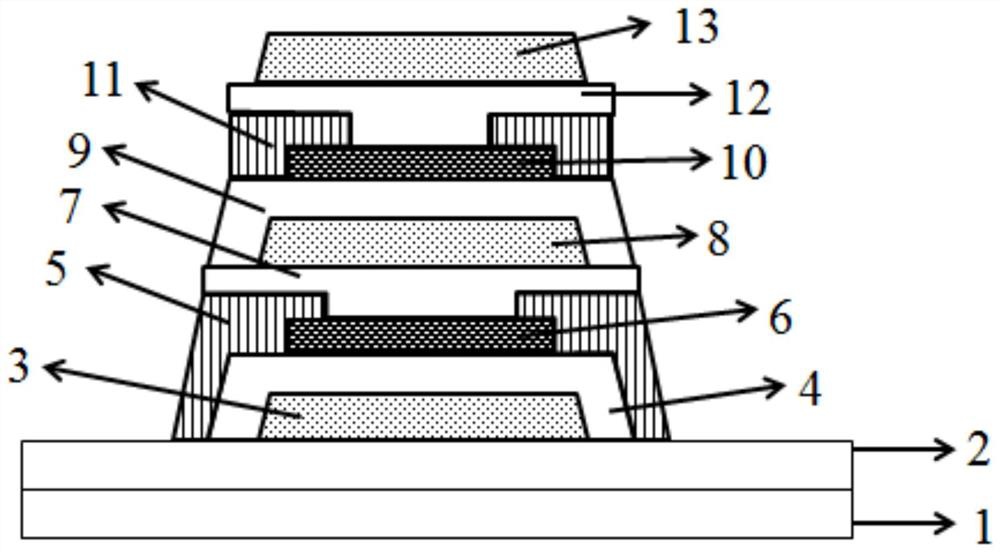
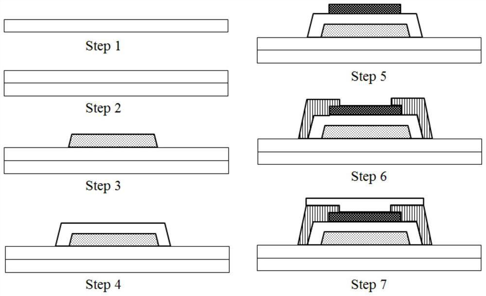
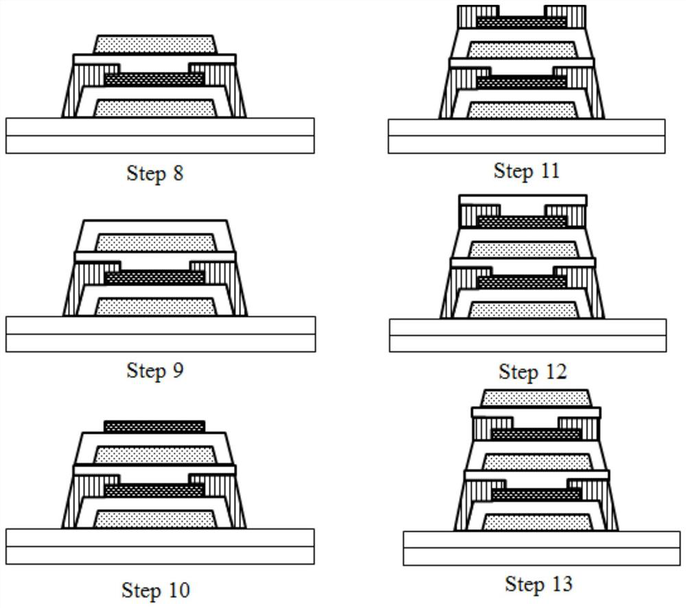
[0030] The preparation of ITO FET see figure 1 and figure 2 :

[0031] The first step: the substrate 1 is Si(111), and the particles, organic matter, oxides, etc. on the substrate are cleaned by a standard RCA cleaning process. After cleaning, the high-purity nitrogen gas is blown dry for use.

[0032]Second step: at first with hydrofluoric acid: the solution of deionized water=1:4 (volume ratio) cleans Si (111) substrate 1, to remove the SiO of surface 2 , and then use...


PUM

PropertyMeasurementUnit
thicknessaaaaaaaaaa
thicknessaaaaaaaaaa
thicknessaaaaaaaaaa

Abstract

The invention discloses a vertical stacking complementary field effect transistor and a preparation method thereof. The n-type indium tin oxide field effect transistor (ITO FET) is located on the bottom layer, the p-type two-dimensional material field effect transistor is located on the upper layer, and the n-type indium tin oxide field effect transistor and the p-type two-dimensional material field effect transistor are vertically stacked to form the complementary field effect transistor, so that the CMOS device which is low in power consumption, small in unit area occupation, small in parasitic effect and high in working speed is obtained.

Description

technical field [0001] The invention belongs to the technical field of semiconductor devices, and in particular relates to a vertically stacked complementary field-effect transistor based on indium tin oxide / two-dimensional material and a preparation method thereof. Background technique [0002] The flat panel display industry has become one of the "core pillar industries" in the field of electronic information in my country. The flat panel display technology can be divided into passive matrix drive and active matrix drive in terms of driving methods. , The core method of high-definition flat panel display. The thin film transistor (TFT), as a driving unit, occupies a very important position in flat panel display technology, and is the key to realize high-resolution display. With the development of flat panel display technology in the direction of high resolution, high response speed, and flexible display, the performance requirements of TFT are also getting higher and highe...

Claims


Application Information

Patent Timeline
Patent Type & Authority Applications(China)
IPC IPC(8): H01L27/092H01L21/8238
CPCH01L27/0922H01L21/823871
Inventor 吴燕庆熊雄胡倩澜童安宇
Owner BEIJING SUPERSTRING ACAD OF MEMORY TECH
Features
  • R&D
  • Intellectual Property
  • Life Sciences
  • Materials
  • Tech Scout
  • Unparalleled Data Quality
  • Higher Quality Content
  • 60% Fewer Hallucinations
Learn More