Traveling wave type cross-octave power amplifier for suppressing harmonic waves in working frequency band
A technology of power amplifier and working frequency band, applied in power amplifiers, radio frequency amplifiers, amplifiers with semiconductor devices/discharge tubes, etc. , high inhibition, easy to achieve effect
- Summary
- Abstract
- Description
- Claims
- Application Information
AI Technical Summary
Problems solved by technology
Method used
Image
Examples
Embodiment 1
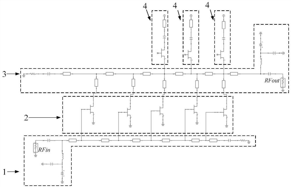
[0032] image 3 It is a schematic diagram of Embodiment 1 of the present invention applied in 6-18GHz. The simulation software is ADS, and the dielectric constant, material parameters, and layer thickness are set according to the GaN HEMT process parameters of the 55th Research Institute of China Electronics Technology Group Corporation. The amplifier core 2 and switch adopt the model of the 55th Research Institute of China Electronics Technology Group Corporation. The entire circuit is provided on a GaN substrate. The gate bias circuit 1-2 and the drain bias circuit 3-4 are connected in series with a large inductor and parallel to the ground with a large capacitor to provide -2V gate voltage and 28V drain voltage respectively. The number of amplifier cores 2 is five, the total gate width is gradually increased from 6*80um to 6*100um, and the common source connection is adopted. The gates of the amplifier core 2 are connected to the gate transmission line 1-3 at equal interv...
Embodiment 2
[0034] Embodiment 2 is different from Embodiment 1 in that a two-stage traveling wave amplification structure is used to increase the amplifier gain, such as Figure 6 mentioned. The whole circuit is set on the GaN substrate, and the drain line 3a is not only the drain line of the pre-amplifier, but also the gate line of the post-amplifier. The gate line 1 is provided with a radio frequency input port 1-1, a gate bias circuit 1-2, and a gate transmission line 1-3, and the gate bias circuit 1-2 provides a die gate voltage of -2V. The drain lines 3a-3b are all provided with a drain transmission line load 3-1, an output compensation inductance 3-2, a drain transmission line 3-3, a drain bias circuit 3-4, and a radio frequency output port 3-5 (the drain line 3a default). Drain line 3a supplies +28V and drain line 3b supplies +56V. The number of amplifier cores 2a is five, the common source connection is adopted, the gates are connected to the gate line 1 at equal intervals, and...
PUM
 Abstract
Description
Claims
Application Information


