Eureka AIR delivers breakthrough ideas for toughest innovation challenges, trusted by R&D personnel around the world.

Semiconductor memory, ferroelectric field effect transistor, and ferroelectric film capacitor

A technology of electric field effect and ferroelectric thin film, applied in the direction of semiconductor devices, semiconductor/solid-state device manufacturing, electric solid-state devices, etc., can solve problems such as ferroelectric fatigue, affect the performance of field-effect transistors or semiconductor memory, and improve anti-fatigue performance , reducing the effect of charge trapping

Active Publication Date: 2022-04-05
XIANGTAN UNIV
View PDF13 Cites 0 Cited by
  • Summary
  • Abstract
  • Description
  • Claims
  • Application Information

AI Technical Summary

Problems solved by technology

However, in practical applications, the inventors of the present application have found that after a period of use of field effect transistors or semiconductor memories based on ferroelectric thin films, the ferroelectric layer usually suffers from relatively serious fatigue problems, that is, "ferroelectric fatigue", The so-called ferroelectric fatigue refers to the state in which the reversible polarization of ferroelectrics gradually decreases after multiple polarization inversions, thus affecting the performance of field effect transistors or semiconductor memories.

Method used

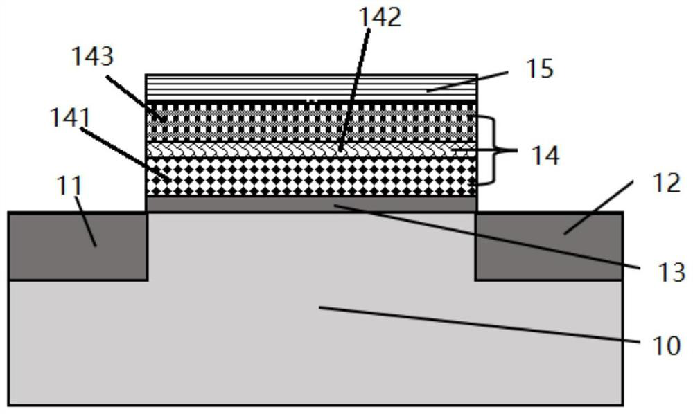
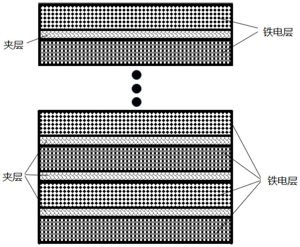
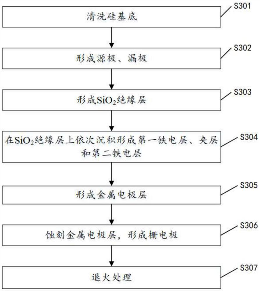

Image

  • Semiconductor memory, ferroelectric field effect transistor, and ferroelectric film capacitor
  • Semiconductor memory, ferroelectric field effect transistor, and ferroelectric film capacitor
  • Semiconductor memory, ferroelectric field effect transistor, and ferroelectric film capacitor

Examples


Embodiment Construction

[0021] In order to make the technical problems, technical solutions and beneficial effects to be solved by the present invention clearer and clearer, the present invention will be further described in detail below in conjunction with the accompanying drawings and embodiments. It should be understood that the specific embodiments described here are only for explaining the present invention, and are not intended to limit the present invention.

[0022] In the following description, use of suffixes such as 'module', 'part' or 'unit' for denoting elements is only for facilitating description of the present invention and has no specific meaning by itself. Therefore, 'module', 'part' or 'unit' may be used in combination.

[0023] It should be noted that the terms "first" and "second" in the description and claims of the present invention and the above drawings are used to distinguish similar objects, but not necessarily used to describe a specific sequence or sequence.

[0024] The...


PUM

PropertyMeasurementUnit
sizeaaaaaaaaaa
sizeaaaaaaaaaa
sizeaaaaaaaaaa

Abstract

The embodiment of the invention discloses a semiconductor memory, a ferroelectric field effect transistor and a ferroelectric film capacitor. The ferroelectric field effect transistor comprises a substrate, a source electrode, a drain electrode, an insulating layer, a first ferroelectric layer, an interlayer, a second ferroelectric layer and a grid electrode layer, the source electrode and the drain electrode are formed in the substrate, the insulating layer is located on the substrate, the projection of the insulating layer is located between the source electrode and the drain electrode, and the first ferroelectric layer, the interlayer, the second ferroelectric layer and the grid electrode layer are sequentially arranged on the insulating layer. The conduction band bottom of the interlayer is higher than or equal to the conduction band bottoms of the first ferroelectric layer and the second ferroelectric layer, and the difference between the conduction band bottoms is smaller than or equal to 0.3 eV. The valence band top of the interlayer is lower than or equal to the valence band tops of the first ferroelectric layer and the second ferroelectric layer, and the difference between the valence band tops of the first ferroelectric layer and the second ferroelectric layer is smaller than or equal to 0.3 eV. According to the embodiment of the invention, charge trapping is inhibited through energy band engineering, so that the anti-fatigue characteristic of the ferroelectric layer can be improved, and the performance of a corresponding element is improved.

Description

technical field [0001] The invention relates to the field of semiconductor storage, in particular to a semiconductor storage, a ferroelectric field effect transistor and a ferroelectric film capacitor. Background technique [0002] Ferroelectric film refers to a film material with ferroelectricity and a thickness of several nanometers to several microns, which is an important class of functional film materials; the so-called "ferroelectricity" refers to the structure of the unit cell in some dielectric crystals. The electric dipole moment appears when the positive and negative charge centers do not coincide, and the electrical polarization intensity is not equal to zero, so that the crystal has spontaneous polarization, and the direction of the electric dipole moment can be changed by an external electric field, showing characteristics similar to ferromagnets , This property of crystals is called ferroelectricity. [0003] In new semiconductor memories, ferroelectric thin f...

Claims


Application Information

Patent Timeline
Patent Type & Authority Applications(China)
IPC IPC(8): H01L29/78H01L49/02H01L29/51H01L27/1159H01L21/336H10N97/00
Inventor 曾斌建谢世昌廖敏彭强祥杨琼周益春
Owner XIANGTAN UNIV
Why Eureka
Eureka Blog
Learn More