A kind of light-emitting diode and its preparation method

A technology of light-emitting diodes and light-emitting layers, which is applied to semiconductor devices, electrical components, circuits, etc., can solve the problems of low overlap rate of electron-hole wave functions and affect the luminous efficiency of light-emitting diodes, so as to improve luminous efficiency and improve electron-hole Effect of hole wave function overlap rate and reduction of migration rate

Active Publication Date: 2022-05-24
JIANGXI ZHAO CHI SEMICON CO LTD
View PDF13 Cites 0 Cited by
  • Summary
  • Abstract
  • Description
  • Claims
  • Application Information

AI Technical Summary

Problems solved by technology

[0005] Aiming at the deficiencies of the prior art, the object of the present invention is to provide a light-emitting diode and its preparation method, aiming at solving the technical problem that the electron-hole wave function overlap rate in the quantum well is low in the prior art, which affects the luminous efficiency of the light-emitting diode

Method used


Image

  • A kind of light-emitting diode and its preparation method
  • A kind of light-emitting diode and its preparation method
  • A kind of light-emitting diode and its preparation method

Examples


Embodiment 1

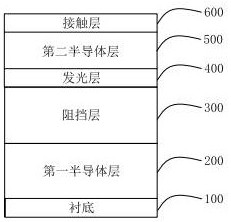
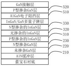
[0034] see Figure 1-Figure 2 , which is a light-emitting diode provided by the first embodiment of the present invention, the light-emitting diode includes a substrate 100; Layer 500 and contact layer 600; wherein, substrate 100, also known as substrate, is a substrate for epitaxial layer growth, used to support and fix the epitaxial layer, substrate 100 can be patterned or non-patterned flat substrate 100 , the characteristics matching between the substrate 100 and the epitaxial layer needs to be very strict, otherwise the growth quality of the epitaxial layer will be affected. At present, the industrialized substrate 100 of light-emitting diodes mainly includes sapphire (Al 2 O 3 ), SiC and Si, different substrate 100 materials, the growth, processing and packaging of light emitting diode structures require different techniques. In this embodiment, sapphire (Al 2 O 3 ) as the substrate 100, sapphire (Al 2 O 3 ) as the most widely used substrate 100 material for light...

Embodiment 2

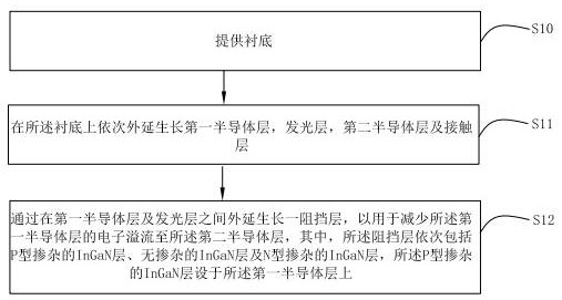
[0050] see image 3 , which shows a method for preparing a light-emitting diode according to the second embodiment of the present invention, and the method includes steps S10-S12:

[0051] Step S10, providing a substrate;

[0052] Among them, the substrate can be a patterned or non-patterned flat substrate, and the characteristics of the substrate and the epitaxial layer must be very strict. For example, lattice mismatch and thermal mismatch need to be matched to grow epitaxial layers with excellent quality. Otherwise, the growth quality of the epitaxial layer and the performance of the light-emitting diode will be directly affected. In this embodiment, the substrate is made of sapphire (Al 2 O 3 ) material, its chemical properties are stable, it does not absorb visible light, it is cheap and low in cost, and its production technology is mature and simple. It is the most widely used substrate material for light-emitting diodes.

[0053] Step S11, sequentially epitaxially g...


PUM

PropertyMeasurementUnit
thicknessaaaaaaaaaa
thicknessaaaaaaaaaa
thicknessaaaaaaaaaa

Abstract

The invention discloses a light-emitting diode and a preparation method thereof, and relates to the technical field of light-emitting diodes. The light-emitting diode comprises: a substrate; a first semiconductor layer, a light-emitting layer, a second semiconductor layer and a contact layer sequentially arranged on the substrate; The barrier layer arranged between the first semiconductor layer and the light-emitting layer is used to reduce the overflow of electrons from the first semiconductor layer to the second semiconductor layer. The barrier layer sequentially includes a P-type doped InGaN layer, an undoped InGaN layer layer and an N-type doped InGaN layer, and a P-type doped InGaN layer is arranged on the first semiconductor layer. The invention can solve the technical problem in the prior art that the electron-hole wave function overlap rate in the quantum well is low, which affects the luminous efficiency of the light-emitting diode.

Description

technical field [0001] The invention relates to the technical field of light emitting diodes, in particular to a light emitting diode and a preparation method thereof. Background technique [0002] With the continuous development and progress of semiconductor technology, as a light-emitting device, light-emitting diodes are more and more widely used in the fields of lighting and displays, and gradually replace the light source of incandescent lamps. Light-emitting diodes, or LEDs for short, emit light through the recombination of electrons and holes, which can efficiently convert electrical energy into light energy. Compared with traditional lamps, the energy consumption of light-emitting diodes is one tenth of that of incandescent lamps, and light-emitting diodes do not contain any heavy metal materials, which is energy-saving and environmentally friendly. It lights up immediately, while ordinary lamps can only be illuminated after they are completely heated after being po...

Claims


Application Information

Patent Timeline
Patent Type & Authority Patents(China)
IPC IPC(8): H01L33/14H01L33/00
Inventor 胡加辉刘春杨金从龙顾伟
Owner JIANGXI ZHAO CHI SEMICON CO LTD
Why Eureka
Try Eureka