Integrated circuit packaging module, preparation method thereof and photoelectric processing module

A technology for encapsulating modules and integrated circuits, applied in circuits, electrical components, electrical solid devices, etc., can solve the damage of photo-induced active surface structure, the low degree of cleanliness of the preset cavity, and affect the transmission efficiency and transmission quality of photonic signals. and other problems to achieve the effect of improving coupling quality and high cleanliness

Active Publication Date: 2022-04-15
JCET SEMICON (SHAOXING) CO LTD
View PDF5 Cites 1 Cited by
  • Summary
  • Abstract
  • Description
  • Claims
  • Application Information

AI Technical Summary

Problems solved by technology

[0004]In the prior art, the high-density heat of the laser is usually used to achieve the melting of a specific area, so as to prepare the required preset cavity, but the high-heat process of the laser It will have adverse effects on the circuits such as transistors in the chip; in addition, the high-density heat of the laser will generate thermal stress in the

Method used


Image

  • Integrated circuit packaging module, preparation method thereof and photoelectric processing module
  • Integrated circuit packaging module, preparation method thereof and photoelectric processing module
  • Integrated circuit packaging module, preparation method thereof and photoelectric processing module

Examples


Example Embodiment

[0045] Next, the technical solutions in the embodiments of the present invention will be described in connection with the drawings of the embodiments of the present invention, and it is understood that the described embodiments are merely the embodiments of the present invention, not all of the embodiments. Based on the embodiments of the present invention, all other embodiments obtained by those of ordinary skill in the art are in the range of the present invention without making creative labor premise.

[0046] In order to make the objects, technical solutions and advantages of the present invention, the present invention will be described in detail below with reference to the accompanying drawings and examples. It is to be understood that the specific embodiments described herein are intended to explain the present invention and is not intended to limit the invention.

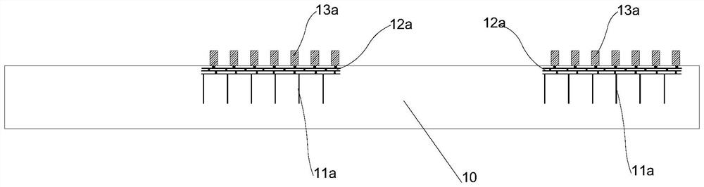
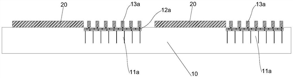
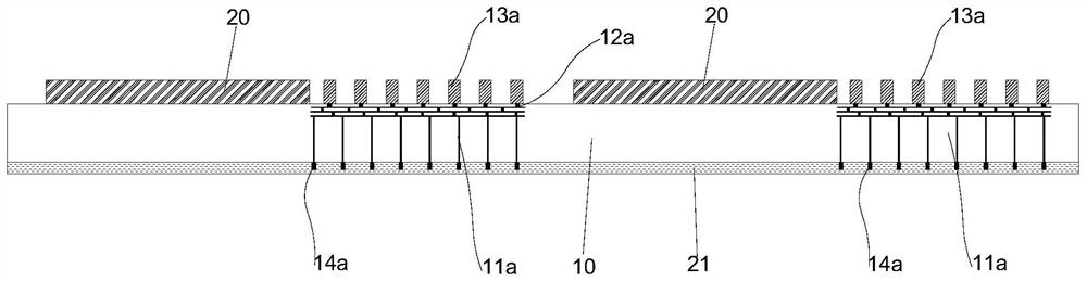
[0047] First aspect, such as Figure 1 to 13 As shown in one embodiment, the present invention provides a meth...


PUM


Abstract

The invention provides a preparation method of an integrated circuit packaging module. The preparation method comprises the following steps: preparing a PIC chip of which a light-induced active surface is coated with a first photoresist layer; cleaning the first photoresist layer, and coating a coating area of the first photoresist layer for multiple times to obtain a second photoresist layer with the thickness being the target thickness; interconnection between the PIC chip and at least one related chip in the multiple related chips and interconnection between the multiple related chips are completed, and a chip module is obtained; performing plastic packaging on the chip module to obtain a first plastic packaging layer, and grinding and thinning the first plastic packaging layer until the second photoresist layer is exposed; and cleaning the second photoresist layer to obtain a preset cavity for laying the optical fiber array waveguide device. The invention also provides an integrated circuit packaging module and a photoelectric processing module. A low-temperature packaging process is adopted, so that adverse effects on circuits such as transistors in the chip are avoided; the preset cavity with relatively high cleanliness can be obtained; and a photoinduced active surface with a complete structure can be obtained.

Description

technical field [0001] The invention relates to the technical field of integrated circuit module packaging, in particular to an integrated circuit packaging module, a preparation method thereof, and a photoelectric processing module. Background technique [0002] As an information carrier, photons have a faster transmission rate than electrons; and there is almost no interference between photons, and photons of different wavelengths, polarizations, and modes can communicate in multiple ways at the same time, so photons have a larger information transmission bandwidth and more High information transmission rate, and not subject to electromagnetic field interference. At present, silicon optoelectronic chips are the information transmission and information processing chip technology with the greatest market development potential. [0003] The microwave light source generated by the laser is coupled to the photonic integrated chip (Photonic Integrated Circuit, PIC) through the ...

Claims


Application Information

Patent Timeline
IPC IPC(8): H01L21/50H01L21/56H01L25/18H01L23/31G02B6/12
Inventor 吴世豪李宗怿郭良奎丁晓春童飞刘籽余
Owner JCET SEMICON (SHAOXING) CO LTD
Why Eureka
Try Eureka