Method for growing silicon oxide thick film by adopting TEOS source PECVD

A technology of silicon oxide and thick film, which is applied in the fields of electrical components, semiconductor/solid-state device manufacturing, circuits, etc., and can solve the problems of growth rate limitation, difficulty in obtaining silicon oxide film, thick film brittleness, etc.

Inactive Publication Date: 2004-03-31
INST OF SEMICONDUCTORS - CHINESE ACAD OF SCI
View PDF0 Cites 0 Cited by
  • Summary
  • Abstract
  • Description
  • Claims
  • Application Information

AI Technical Summary

Problems solved by technology

However, the ordinary CVD method is limited by the growth rate on the one hand, and on the other hand, due to the influence of the quality of the grown silicon oxide film, it is prone to embrittlement of the thick film, so it is difficult to obtain a silicon oxide film with a thickness exceeding 10 microns.

Method used


Image

  • Method for growing silicon oxide thick film by adopting TEOS source PECVD
  • Method for growing silicon oxide thick film by adopting TEOS source PECVD
  • Method for growing silicon oxide thick film by adopting TEOS source PECVD

Examples


Embodiment Construction

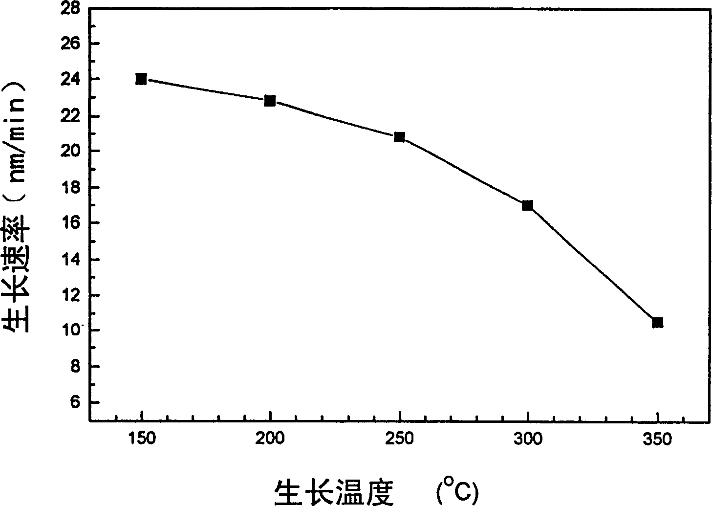
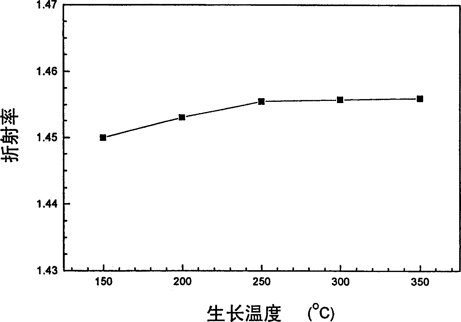
[0014] Table 1 Reaction conditions for silicon oxide growth by TEOS-PECVD

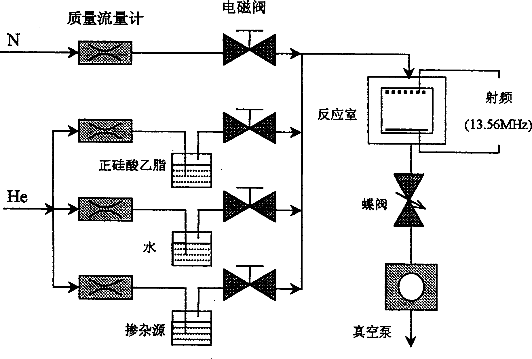
[0015] A two-inch monocrystalline silicon wafer is selected, the surface of the silicon wafer is cleaned according to a conventional cleaning process, and then placed in the reaction chamber after being spin-dried, the reaction chamber is vacuumed to the background vacuum, and the substrate is heated. Heat the source in advance so that TEOS and H 2 O is kept at a constant temperature (30~50℃; 20~30℃). Use He as the carrier gas, and use the bubbling method to combine TEOS and H 2 O was carried into the reaction chamber, and the radio frequency was started. The deposition conditions are shown in Table 1.

[0016] The liquid source is combined with the conventional PECVD technology to prepare the material, and the method used is completely compatible with the current Si integration process. H 2 O-TEOS plasma CVD technology applies the principle of plasma enhancement when forming silicon oxid...


PUM

PropertyMeasurementUnit
thicknessaaaaaaaaaa

Abstract

The invention relates to a method to grow silicon oxide thick film by using TEOS source PECVD. The surface of silicon wafer is cleaned, then the silicon wafer is put into a reaction chamber. The TESO and H2O are carried into the reaction chamber by using bubble-fixation method with He being as carrying gas. The TESO is kept at constant temperature 30 degree C-50 degree C and H2O at 20 degree C-30 degree C by using method of heating in water bath. The silicon oxide is done with high temperature annealing. The invented method provides good performances of even film thickness (1.5%, at 2 inches substrate, refractive index being controlled within 1.453 plus or minus 0.001, stable refractive index without change after high temperature annealing and it can be used to grow thick film. The total growing technique is compatible to silicon technique.

Description

Technical field [0001] The invention belongs to a semiconductor material, especially a method for growing a thick silicon oxide film. Background technique [0002] Wavelength division multiplexing technology (WDM) is an effective method to solve broadband, large-capacity optical fiber network communication. The multiplexer / demultiplexer is a key component of the WDM system. Practical multiplexing devices have been developed, including interference filters, fiber gratings and planar lightwave circuit devices. However, as the number of channels continues to increase, devices such as interference filters and fiber gratings become extremely complex, and the loss increases rapidly with the increase of the number of channels, resulting in a serious imbalance in channel loss. Planar waveguide multiplexer / demultiplexer based on arrayed waveguide grating (AWG) is the most attractive at this time. Through design, excellent performance such as large number of channels, flat passband respons...

Claims


Application Information

Patent Timeline
Patent Type & Authority Patents(China)
IPC IPC(8): H01L21/316H01L21/324
Inventor 雷红兵王红杰胡雄伟邓晓清王启明
Owner INST OF SEMICONDUCTORS - CHINESE ACAD OF SCI
Why Eureka
Try Eureka