Novel fuse link processing technology

A processing technology and technology of fuse link, which is applied in the field of new fuse link processing technology, can solve problems such as tolerance, difference in shape of fuse structure, difficulty in cutting quality guarantee, etc., achieve high efficiency, reduce production cost, and do not affect the effect of breaking capacity

Inactive Publication Date: 2022-05-06
苏州华德电子有限公司
View PDF1 Cites 0 Cited by
  • Summary
  • Abstract
  • Description
  • Claims
  • Application Information

AI Technical Summary

Problems solved by technology

[0003] At present, there are two methods widely used in the manufacture of fuses, one is the printing and electroplating process, and the other is threading the wire in the cavity. The performance of the fuse manufactured by threading the wire in the cavity is relatively stable, but its production efficiency is low. As a result, the product cost has always been relatively high, and it is difficult to produce small or ultra-small fuses. The printing and plating process provides a method for mass production of fuses. The Chinese patent No. CN101202186A discloses a chip fuse and The manufacturing method specifically refers to cutting the glass-ceramic layer in the width direction to form a slit, and then coating the metal film slurry at least once, the slurry penetrates into the slit, the metal film slurry forms a fuse structure in the cutting slit, and cutting There are tolerances in itself, it is difficult to control the size of the gap, which directly leads to differences in the shape of the fuse structure, the cutting quality is difficult to guarantee, and there is a possibility of disconnection. These factors directly cause damage to the performance of the fuse structure; in addition, the fuse structure is directly related to glass ceramics. When the layers are in contact, the thermal conductivity of the glass-ceramic layer is stronger than that of air. When working, heat will be conducted from the glass-ceramic layer, which will affect the fusing performance.

Method used


Image

  • Novel fuse link processing technology
  • Novel fuse link processing technology
  • Novel fuse link processing technology

Examples


Embodiment Construction

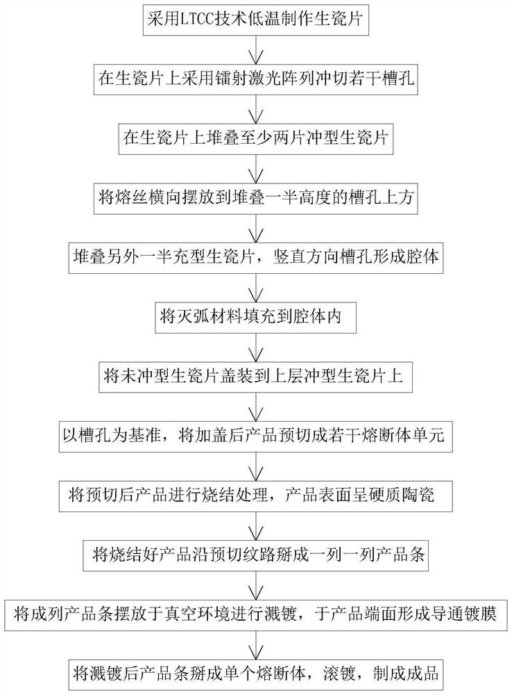
[0036] The preferred embodiments of the present invention will be described in detail below in conjunction with the accompanying drawings, so that the advantages and features of the invention can be more easily understood by those skilled in the art, so as to define the protection scope of the present invention more clearly.

[0037] see Figure 1 to Figure 11 , the embodiment of the present invention includes:

[0038] A novel fuse link processing technology, the novel fuse link processing technology includes the following steps:

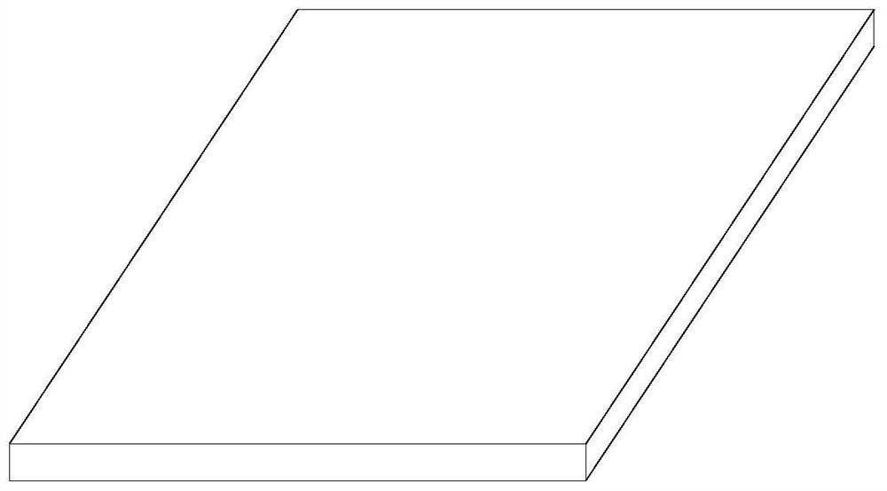
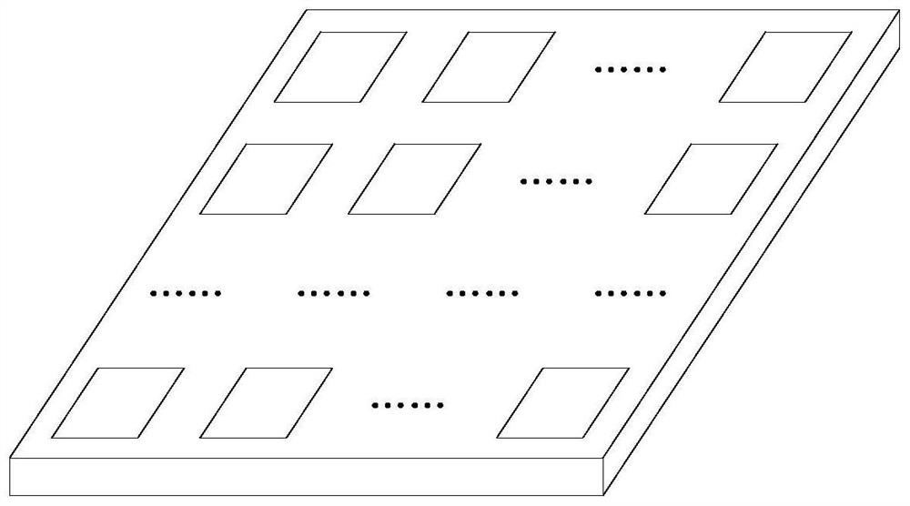
[0039] Step (1) Punching, punching a number of slots on the green ceramic sheet with a laser array, the green ceramic sheet is made by LTCC technology, the thickness of the punching green ceramic sheet is 120mm, and punching in a low temperature environment;

[0040] Step (2) stacking, stacking at least two punched green ceramic sheets on the unpunched green ceramic sheet;

[0041] Step (3) Embedding, when stacking to half the height of the produ...


PUM

PropertyMeasurementUnit
thicknessaaaaaaaaaa

Abstract

The invention discloses a novel fuse link processing technology, which comprises the following steps of: punching: punching a plurality of slotted holes in a green ceramic chip by adopting a laser array; stacking, wherein at least two punching green ceramic chips are stacked on the green ceramic chips; embedding a fuse wire, and transversely placing the fuse wire on the raw ceramic chip above the slotted hole; stacking: remaining half of the height of the raw ceramic chips; filling: filling an arc extinguishing material into a cavity formed in the vertical direction of the slotted hole; covering, namely covering the unpunched green ceramic chip on the punched green ceramic chip on the upper layer; pre-cutting: pre-cutting the capped product into a plurality of fuse link units; sintering: carrying out sintering treatment; stripping, namely breaking off the sintered product into rows of product strips along the pre-cut lines; sputtering coating: sputtering coating is carried out in a vacuum environment, and the end face of the product strip is conducted; stripping particles, breaking off the sputtering product strips into single fuse links, and carrying out barrel plating to prepare a finished product. By means of the mode, multiple finished products can be manufactured at a time, efficiency is high, the fuse is directly buried, the fuse is arranged in the groove hole in a suspended mode, and the breaking capacity is not affected.

Description

technical field [0001] The invention relates to the technical field of electronic protection components, in particular to a novel process for processing fuse links. Background technique [0002] SMD fuse is widely used in printed circuit boards. With the miniaturization of electronic devices, its size is getting smaller and smaller. It is an electrical component installed in the circuit to ensure the safe operation of the circuit. When the circuit occurs When a fault or abnormality occurs, the current will continue to rise, and the rising current may damage some important or valuable devices in the circuit, or burn the circuit or even cause a fire. The fuse protects electronic equipment from overcurrent damage, and also Serious injury caused by internal failure of electronic equipment can be avoided. [0003] At present, there are two methods widely used in the manufacture of fuses, one is the printing and electroplating process, and the other is threading the wire in the c...

Claims


Application Information

Patent Timeline
Patent Type & Authority Applications(China)
IPC IPC(8): H01H69/02
CPCH01H69/02
Inventor 颜睿志
Owner 苏州华德电子有限公司
Why Eureka
Try Eureka