Layout design method for improving ESD (Electro-Static Discharge) protection capability of interdigital structure type device

An interdigital structure and layout design technology, which is applied in the field of layout design to improve the ESD protection ability of interdigital structure devices, can solve the problems affecting the on-chip ESD protection ability of high-voltage circuits, and it is difficult to trigger uniformly, so as to alleviate the current non-uniformity , Improve performance, increase the effect of withstand voltage and current discharge capacity

Pending Publication Date: 2022-05-13
NORTHWEST UNIV
View PDF0 Cites 0 Cited by
  • Summary
  • Abstract
  • Description
  • Claims
  • Application Information

AI Technical Summary

Problems solved by technology

However, high-voltage LDMOS devices exhibit greater snapback than low-voltage MOS devices, and generally the multi-finger uniform trigger condition with failure voltage greater than the trigger voltage cannot be satisfied, and it is more difficult to uniformly trigger than low-voltage multi-finger devices, which directly affects the on-chip of high-voltage circuits. ESD protection ability

Method used


Image

  • Layout design method for improving ESD (Electro-Static Discharge) protection capability of interdigital structure type device
  • Layout design method for improving ESD (Electro-Static Discharge) protection capability of interdigital structure type device
  • Layout design method for improving ESD (Electro-Static Discharge) protection capability of interdigital structure type device

Examples


Embodiment 1

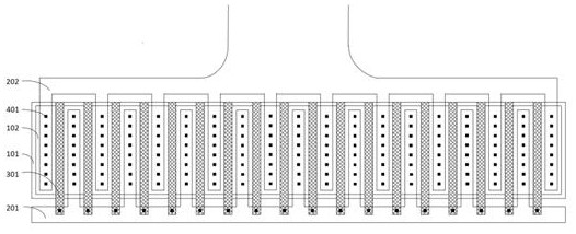
[0036] In order to solve the problems existing in the prior art, the present invention proposes a layout design method for improving the ESD protection capability of interdigitated structure devices. The method of the present invention will be further described below in conjunction with the embodiments, wherein, image 3 It is a schematic diagram of the layout structure of GGNMOS in the interdigitated ESD device; Figure 4 It is a schematic cross-sectional view of GGNMOS in the interdigitated ESD device described in the present invention;

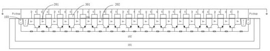
[0037] The schematic diagram of the conventional GGNMOS structure in the ESD protection device is as follows figure 2 As shown, the length of each finger in the source and drain regions is equal, and its structure is an interdigital structure, which has non-uniform current, and may cause permanent damage to the device due to excessive voltage during electrostatic discharge.

[0038] Therefore, a kind of interdigitated GGNMOS device struct...

Embodiment 2

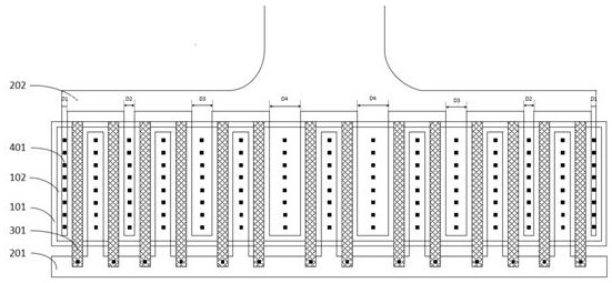
[0048] refer to Image 6 , Image 6 The general multi-finger source-liner connection NMOS device is designed for the layout design method for improving the ESD protection capability of the interdigitated device according to the present invention. Its structure is basically the same as the standard source-lined connection NMOS structure, but the interdigit length D4 of the drain region at the center of the interdigit structure is greater than the interdigit length of the drain region gradually away from the interdigit center, that is, D4>D3>D2>D1. The gate connection method can be any one of routePolydir (top, bottom, both). For the sake of simplicity in the schematic diagram, the gate connection method is not shown.

[0049] In view of the poor reliability of GGNMOS and the shortcomings of general current discharge capability, the present invention can increase the reliability of GGNMOS without affecting the basic parameters of the device itself by only changing the drawing m...


PUM


Abstract

A layout design method for improving the ESD protection capability of an interdigital structure type device is characterized in that on the basis of a traditional interdigital type ESD protection device, the length of a drain region interdigital is increased at the center of an interdigital structure, and according to the fact that the total length of a gate structure and a source structure is not changed, the farther the distance from the center of the interdigital structure is, the farther the distance from the center of the interdigital structure is; and designing the interdigital length of the drain region according to the principle that the interdigital length of the drain region is smaller. Finally, under the condition that the total length of the gate and source structures is not changed and the area is the same, the ESD capability is higher; when the ESD capacity is the same, the area is smaller; the influence of current heterogeneity during ESD protection of the interdigital structure type device is relieved, compared with a traditional interdigital structure device, the MOS device using the method is better in ESD protection capacity, higher in current discharge capacity and higher in reliability, layout modification only needs to be conducted on a chip, and the manufacturing cost is reduced. The performance of the interdigital structure can be improved without influencing the basic parameters of the device, and the ESD protection capability, the reliability and the electrostatic discharge capability of the interdigital structure type device are improved.

Description

technical field [0001] The invention belongs to the field of integrated circuits, and in particular relates to a layout design method for improving the ESD protection capability of an interdigitated device. Background technique [0002] With the development of the manufacturing process of integrated circuits, the feature size of CMOS technology continues to shrink, and the ability of transistors to withstand high voltage and high current continues to decrease. CMOS integrated circuits are more susceptible to failure due to electrostatic shock, resulting in a decline in product reliability. [0003] Static electricity is ubiquitous in the process of chip manufacturing, packaging, testing and use. The accumulated static charge is released in nanoseconds to microseconds with a current of several amperes or tens of amperes. The instantaneous power is as high as hundreds of kilowatts, and the discharge energy It can reach millijoules, and the destruction intensity of the chip is ...

Claims


Application Information

Patent Timeline
IPC IPC(8): G06F30/392
CPCG06F30/392
Inventor 齐晓斐崔珂瑜胡一博钱颢马晓龙张志勇赵武
Owner NORTHWEST UNIV
Why Eureka
Try Eureka