

Silicon-based Schottky photoelectric detector and preparation method and application thereof
A technology of photodetector and Schottky contact, which is applied in the direction of circuits, electrical components, semiconductor devices, etc., can solve the problems of sharp drop in responsivity, unobvious dark current suppression, poor conductivity, etc., achieve large responsivity, increase electrode Light transmission performance, dark current suppression effect
- Summary
- Abstract
- Description
- Claims
- Application Information
AI Technical Summary
Problems solved by technology
Method used
Image

Examples
Embodiment 1
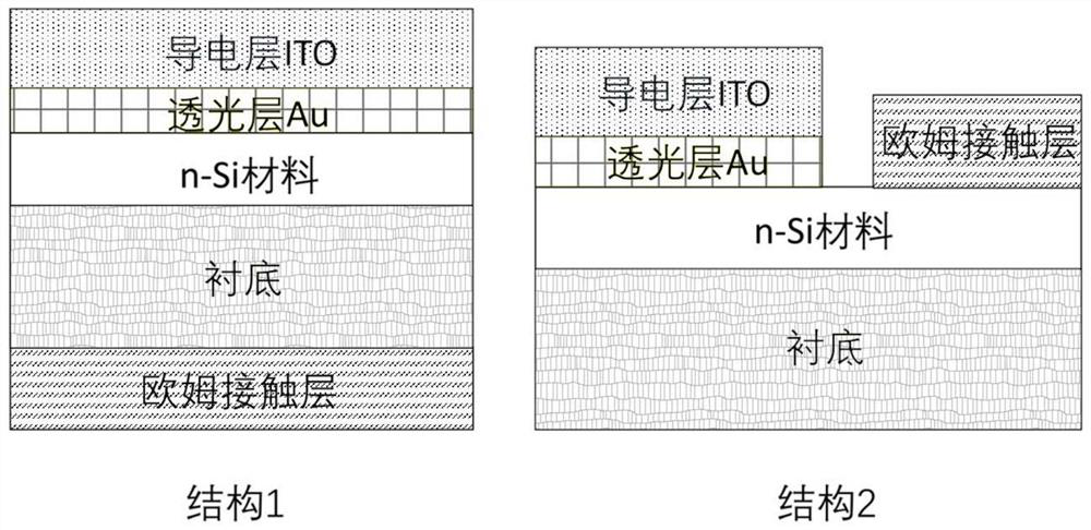
[0083] This embodiment is used to illustrate the structure and preparation method of the silicon-based Schottky photodetector (ITO / 6nmAu / Si / Al) with an Au insertion layer of the present invention.
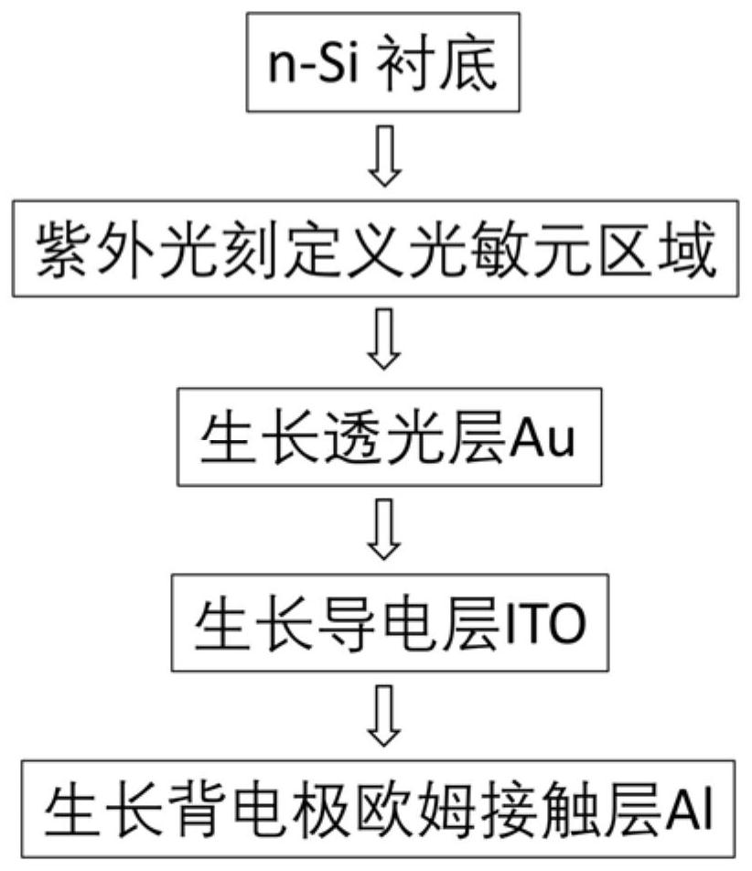
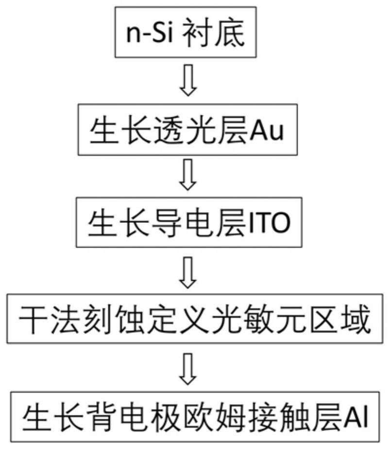
[0084] Specifically, in this scheme, the device structure is selected as the attached figure 1 Structure in 1. The substrate is a commercial epi-readyn type silicon substrate (0.1~1Ω-cm, thickness 400±10μm); the photosensitive element is defined by ultraviolet lithography, and the area is selected as 0.02cm 2 ; The light-transmitting layer used to improve the Schottky barrier is selected as a 6nm Au film grown by electron beam evaporation; the conductive electrode is selected as a 100nm ITO film material grown by magnetron sputtering; the back ohmic contact electrode is selected as a 300nm Al film grown by electron beam evaporation .
[0085] In this embodiment, the Schottky semiconductor material layer is directly selected as the n-type silicon substrate material, and no new Sch...
Embodiment 2
[0089] This embodiment is used to illustrate the structure and preparation method of the silicon-based Schottky photodetector (ITO / 6nmAu / Si / Al) with an Au insertion layer of the present invention.
[0090] Specifically, in this scheme, the device structure is selected as the attached figure 1 Structure in 1. The substrate is a commercial epi-readyn type silicon substrate (0.1~1Ω-cm, thickness 400±10μm); the photosensitive element is defined by ultraviolet lithography, and the area is selected as 0.0007cm 2 ; The light-transmitting layer used to improve the Schottky barrier is selected as a 6nm Au film grown by electron beam evaporation; the conductive electrode is selected as a 100nm ITO film material grown by magnetron sputtering; the back ohmic contact electrode is selected as a 300nm Al film grown by electron beam evaporation .
[0091] In this embodiment, the Schottky semiconductor material layer is directly selected as the n-type silicon substrate material, and no new S...
Embodiment 3
[0095] This example is used to illustrate the structure and preparation method of the silicon-based Schottky photodetector (ITO / 2nmAu / Si / Al) with an Au insertion layer of the present invention.
[0096] Specifically, in this scheme, the device structure is selected as the attached figure 1 Structure in 1. The substrate is a commercial epi-readyn type silicon substrate (0.1~1Ω-cm, thickness 400±10μm); the photosensitive element is defined by ultraviolet lithography, and the area is selected as 0.0007cm 2 ; The light-transmitting layer used to improve the Schottky barrier is selected as a 2nm Au film grown by electron beam evaporation; the conductive electrode is selected as a 100nm ITO film material grown by magnetron sputtering; the back ohmic contact electrode is selected as a 300nm Al film grown by electron beam evaporation .
[0097] In this embodiment, the Schottky semiconductor material layer is directly selected as the n-type silicon substrate material, and no new Scho...
PUM
| Property | Measurement | Unit |
|---|---|---|
| thickness | aaaaa | aaaaa |
| thickness | aaaaa | aaaaa |
| thickness | aaaaa | aaaaa |
Abstract
Description
Claims
Application Information