Filter fan-out packaging structure and manufacturing method thereof

A technology of packaging structure and manufacturing method, applied in impedance network, electrical components and other directions, can solve the problems affecting yield, strict flatness requirements of substrate and sealing cover, high split rate, etc., to improve yield and reliability, The effect of avoiding the influence of photolithography offset and enhancing the molding resistance

Pending Publication Date: 2022-05-17
XIAMEN SKY SEMICON TECH CO LTD
View PDF0 Cites 0 Cited by
  • Summary
  • Abstract
  • Description
  • Claims
  • Application Information

AI Technical Summary

Problems solved by technology

[0004] 1. The cost of the surface sealing cover is relatively high;
[0005] 2. The reliability of the product has strict requirements on the flatness of the substrate and the sealing cover, which is easy to cause failure
[0006] 3. The thickness of the existing package is relatively thick, which does not meet the requirements of the current miniaturization trend of radio frequency devices
[0007] 4. The film-covered package on the surface of the device is sensitive to the size of the first cavity, and it is easy to cause film collapse in a large cavity size to affect the performance of the chip;
[0008] 5. At present, wafer-level packaging is mainly concentrated in 4 / 6 inches due to the ultra-thin LT wafer, and there is a high split rate, which affects the yield rate
[0009] Fan-out packaging of SAW devices can effectively solve and improve the above problems, but one of the challenges faced by fan-out packaging technology is chip offset, which brings difficulties to the alignment of subsequent photolithography processes

Method used


Image

  • Filter fan-out packaging structure and manufacturing method thereof
  • Filter fan-out packaging structure and manufacturing method thereof
  • Filter fan-out packaging structure and manufacturing method thereof

Examples


Embodiment 1

[0050] refer to Figures 1a-1h , the embodiment of the present application proposes a method for manufacturing a filter fan-out packaging structure, including the following steps:

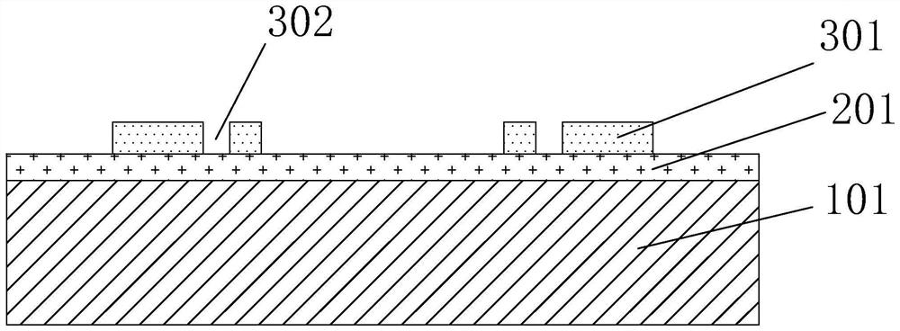
[0051] (1) Reference Figure 1a , providing a carrier wafer 101, the surface of the carrier wafer 101 is covered with an adhesive layer 201 with a thickness of about 100um, the material of the adhesive layer 201 is a thermal foaming film, and the thickness of the adhesive layer 201 is made to be about 5- The barrier layer 301 is 50um. The material of the barrier layer 301 is bondable photoresist or dry film. The barrier layer 301 is patterned to form the second through hole 302. The patterning process includes a photolithography process. By setting the second through hole 302 on the barrier layer 301 to form an alignment structure, the position of the second through hole 302 corresponds to the pad of the filter chip, so that when the filter chip is aligned on the carrier wafer 101 The second throu...

Embodiment 2

[0059] refer to Figure 2a-2e , the embodiment of the present application proposes a method for manufacturing a filter fan-out packaging structure, including the following steps:

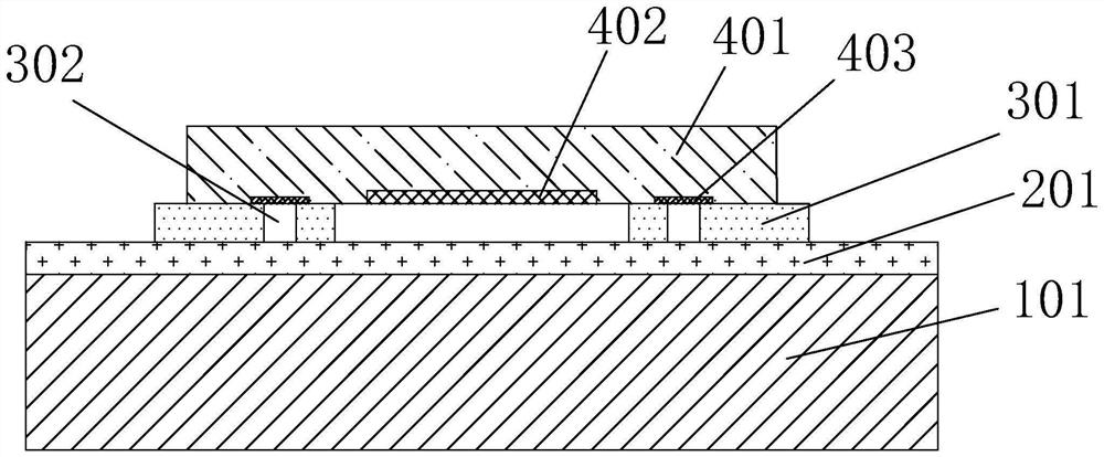
[0060] (1) Reference Figure 2a , provide a carrier wafer 111, the surface of the carrier wafer 111 is covered with an adhesive layer 211 with a thickness of about 100um, the material of the adhesive layer 211 is a thermal foaming film, and the thickness of the adhesive layer 211 is 25-50um The barrier layer 311 is made of a bondable photoresist or dry film, and the barrier layer 311 is patterned to form the second through hole 312. The patterning process includes a photolithography process. The alignment structure is formed by setting the second through hole 312 on the barrier layer 311. The position of the second through hole 312 corresponds to the pad of the filter chip 411 on which the first spacer layer 414 has been formed, so that the filter chip is aligned. The second through hole 312 is lo...

Embodiment 3

[0068] refer to Figures 3a-3i , the embodiment of the present application proposes a method for manufacturing a filter fan-out packaging structure, including the following steps:

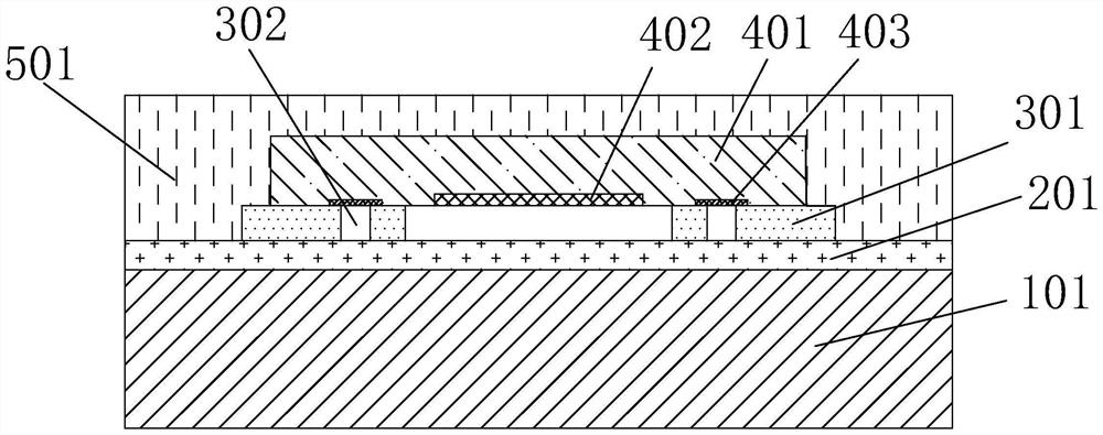
[0069] (1) Reference Figures 3a-3c Provide a carrier wafer 121, the surface of the carrier wafer 121 is covered with an adhesive layer 221 with a thickness of about 100um, the material of the adhesive layer 221 is a thermal foam film, and the position corresponding to the pad on the adhesive layer 211 is set There is an alignment block 322, and a barrier layer 321 with a thickness of 25-50um is made around the alignment block 322 above the adhesive layer 221. The barrier layer 321 is first made on the adhesive layer 221 and covers the alignment block 322, The barrier layer 321 is planarized so that the surface of the barrier layer 321 is flush with the surface of the alignment block 322 . Specifically, the material of the barrier layer 321 is photoresist, molding material or dry film, and the al...


PUM


Abstract

The invention discloses a filter fan-out packaging structure and a manufacturing method thereof, a filter chip comprises a resonance area and a non-resonance area outside the resonance area, a bonding pad is arranged on the non-resonance area, a bonding layer covers the surface of an additionally provided carrier plate wafer, a barrier layer is manufactured above the bonding layer, and the barrier layer is arranged on the surface of the carrier plate wafer. An alignment structure is formed on an enclosure layer or a non-resonance area, the position of the alignment structure corresponds to a bonding pad, a filter chip is attached to a carrier plate wafer in an alignment mode through the alignment structure so as to form a first cavity above a resonance area, and the back face and the side face of the filter chip and the back face and the side face of the enclosure layer are covered with a plastic package layer. And removing the carrier wafer and the bonding layer, manufacturing a protective layer on the enclosure layer, and arranging a metal connecting structure and a solder ball through a first through hole in the protective layer and the alignment structure. According to the invention, the problems of offset of fan-out packaging of the filter chip and LT wafer cracking can be solved, the mold pressing resistance of the cavity structure is effectively enhanced, the production cost is reduced, and ultrathin packaging is realized.

Description

technical field [0001] The invention relates to the field of filter packaging, in particular to a filter fan-out packaging structure and a manufacturing method thereof. Background technique [0002] With the rapid development of the communication field, since the filter plays an important role in the communication field, new progress is constantly being made. As a frequency selection device, the filter can pass specific frequency components in the signal and greatly attenuate other frequency components. In the field of modern communication technology, there is almost no branch that is not affected by filtering technology. Filters are widely used in source coding, channel coding, modulation, multiplexing, data compression, and adaptive channel equalization, especially in applications such as digital communication, network communication, and image communication. It was almost impossible to move an inch. [0003] At present, the main packaging technology of filters is still ...

Claims


Application Information

Patent Timeline
Patent Type & Authority Applications(China)
IPC IPC(8): H03H9/10H03H3/08
CPCH03H9/1064H03H3/08
Inventor 黄剑洪姜峰于大全
Owner XIAMEN SKY SEMICON TECH CO LTD
Why Eureka
Try Eureka