Semiconductor device with saturation current self-clamping function and preparation method thereof
A saturation current and semiconductor technology, which is applied in the field of power semiconductor devices with saturation current self-clamping function and its preparation, can solve the problem of increasing the on-state voltage drop of IGBT devices, increasing the on-state loss of devices, and affecting the electronic current of IGBT devices and other problems, to achieve the effect of self-shutdown of the device, improvement of short-circuit capability, and practicability
- Summary
- Abstract
- Description
- Claims
- Application Information
AI Technical Summary
Problems solved by technology
Method used
Image

Examples
Embodiment 1
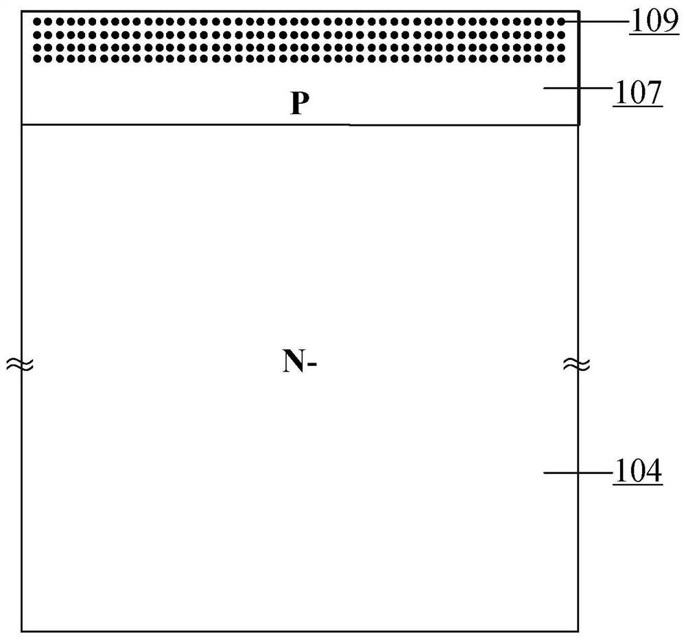
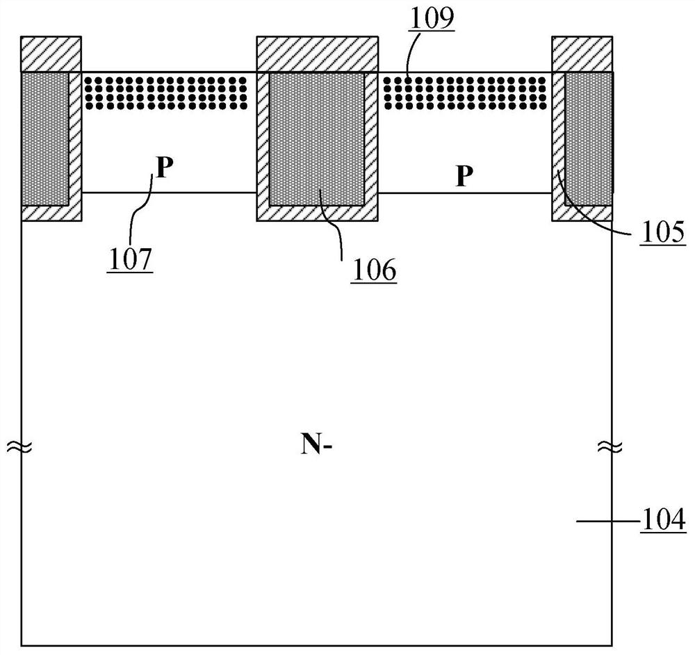
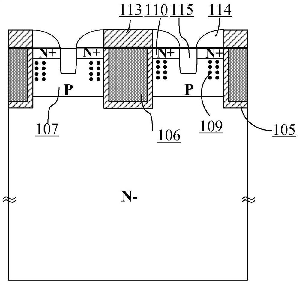
[0035] figure 1 It is a schematic cross-sectional view 100 of an IGBT device according to the first embodiment of the present invention, a self-clamping function IGBT structure with saturation current, the device structure has: a semiconductor chip 100 includes a first collector 101 at the bottom, a first P Type collector region 102 is located above the first collector electrode 101; located above the first field stop layer 103 (or N buffer layer) is the first lightly doped region N - 104, the first lightly doped region N - Just above 104 is a surface MOS structure, the surface MOS structure consists of a first gate oxide layer 105, a first polysilicon gate 106, a first P-type body region 107 and a first heavily doped N + The emitter region 110 is formed; the first emitter metal 112 passes through the first tungsten plug 111 and the first heavily doped region P + 108 connected. In particular, the first heavily doped N + Below the emitter region 110 and close to the first g...
Embodiment 2
[0050] Figure 10 It is a schematic cross-sectional view 200 of the RC-IGBT device according to the second embodiment of the present invention. The device structure has: a second collector 201 at the bottom, and a second N on the top of the second collector 201, respectively. + The heavily doped region 213 and the second P-type collector region 202 are located above the second field stop layer 203 (or the N buffer layer) as the second N - Lightly doped region 204, second N - Just above the lightly doped region 204 is a surface MOS structure, and the surface MOS structure consists of a second gate oxide layer 205 , a second polysilicon gate 206 , a second P-type body region 207 and a second N + The heavily doped emitter region 210 is formed; the second emitter metal 212 passes through the second tungsten plug 211 and the second P + The heavily doped regions 208 are connected. In particular, the second N + Below the heavily doped emitter region 210 and near the second gate ...
Embodiment 3
[0052] Figure 11 It is a schematic cross-sectional view 300 of the SGT device according to the second embodiment of the present invention. The device structure has: a third collector 301 at the bottom, and a third N above the third collector 301 respectively + Heavily doped region 302, located in the third N + Above the heavily doped region 302 is the third N - Lightly doped region 303, third N - Just above the lightly doped region 303 is a surface MOS structure, the surface MOS structure consists of a polysilicon field plate 304, a third gate oxide layer 305, a third polysilicon gate 306, a third P-type body region 307 and a third N + A heavily doped emitter region 310 is formed. The third emitter metal 312 passes through the third tungsten plug 311 and the third P + The heavily doped regions 308 are connected. In particular, the third N + Below the emitter region 310 and near the third gate oxide layer 305, there are third deep level acceptor impurities 309. The thir...
PUM
 Abstract
Description
Claims
Application Information