
One-way carrier photodetector and preparation method thereof

A single-line carrier and photodetector technology, applied in the field of photoelectric detection, can solve the problems of reducing the photoresponse of devices, difficulty in carrier transport, polarization and poor heat dissipation, etc.

Pending Publication Date: 2022-05-27
SOUTH CHINA UNIV OF TECH
View PDF0 Cites 1 Cited by
  • Summary
  • Abstract
  • Description
  • Claims
  • Application Information

AI Technical Summary

Problems solved by technology

However, problems such as internal polarization and poor heat dissipation of the device structure of the single-row carrier photodetector will lead to low saturation linear output of the detector and difficulty in carrier transport. In addition, the traditional structure of the metal electrode will reflect part of the visible light, reducing the device's performance. light response

Method used


Image

  • One-way carrier photodetector and preparation method thereof
  • One-way carrier photodetector and preparation method thereof
  • One-way carrier photodetector and preparation method thereof

Examples


Embodiment

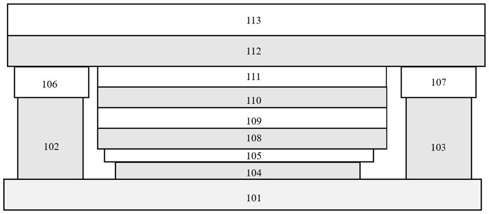
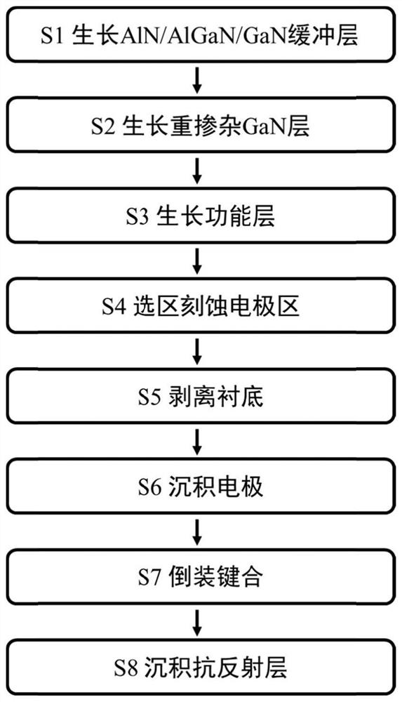
[0059] An embodiment provides a single-line carrier light detector, such as Figures 1 to 3 As shown, the single-line carrier photodetector structure comprises:

[0060] AlN substrate 101; a first metal pad 102, a second metal pad 103 and a third metal pad 104 located on the upper surface of the AlN substrate 101; a first N-type electrode 106 located on the upper surface of the first metal pad 102; a second N-type electrode 107 located on the upper surface of the second metal pad 103; a P-type electrode 105 located on the upper surface of the third metal pad 104; a P-type contact layer 108 located on the upper surface of the P-type electrode 105 The electron barrier layer 109 located on the upper surface of the P-type contact layer 108; the absorption layer 110 located on the upper surface of the electron barrier layer 109; the collection layer 1110 located on the upper surface of the absorption layer 110; the N-type contact layer 112 located on the upper surface of the collection ...


PUM

PropertyMeasurementUnit
thicknessaaaaaaaaaa
thicknessaaaaaaaaaa
thicknessaaaaaaaaaa

Abstract

The invention provides a one-way carrier photodetector and a preparation method thereof. The uni-traveling carrier optical detector structure comprises an AlN substrate; the first metal bonding pad, the second metal bonding pad and the third metal bonding pad are located on the upper surface of the substrate; the first N-type electrode is positioned on the upper surface of the first metal bonding pad; the second N-type electrode is positioned on the upper surface of the third metal bonding pad; the P-type electrode is positioned on the upper surface of the second metal bonding pad; the P-type contact layer is positioned on the upper surface of the P-type electrode; the electron blocking layer is positioned on the upper surface of the P-type contact layer; the collecting layer is positioned on the upper surface of the electron blocking layer; the absorbing layer is positioned on the upper surface of the collecting layer; the N-type contact layer is positioned on the upper surfaces of the absorption layer, the first N-type electrode and the second N-type electrode; the anti-reflection layer is positioned on the upper surface of the N-type contact layer; and the absorption layer is a p-type gradient doped InGaN layer. The uni-traveling carrier photodetector has high saturation linear output and high response rate.

Description

Technical field [0001] The present invention belongs to the field of photoelectric detection technology, in particular to a single-line carrier photodetector and a method for preparing it. Background [0002] With the development of a new generation of wireless communication technology, the huge spectrum resources of the visible light band make visible light communication technology occupy a pivotal position in the new generation of mobile communication technology. As a semiconductor device that converts the detected light signal into an electrical signal, the visible light detector is one of the key devices that determine the advantages and disadvantages of the entire visible light communication system. The new generation of high-speed visible light communication systems puts forward new requirements for the performance of photodetectors, namely: high speed (high bandwidth), high response rate and high saturated output power. [0003] The traditional PIN type light detector show...

Claims


Application Information

Patent Timeline
Patent Type & Authority Applications(China)
IPC IPC(8): H01L31/0304H01L31/105H01L31/02H01L31/0216H01L31/18
CPCH01L31/03048H01L31/03042H01L31/02161H01L31/02005H01L31/105H01L31/1848Y02P70/50
Inventor 李国强陈亮王文樑柴吉星
Owner SOUTH CHINA UNIV OF TECH
Learn More