Novel AC-DC rectifier circuit
A rectifier circuit and a new technology, applied in the field of rectifiers, can solve the problems of low efficiency and high production cost, and achieve the effects of high efficiency, low cost and simple circuit
- Summary
- Abstract
- Description
- Claims
- Application Information
AI Technical Summary
Problems solved by technology
Method used
Image

Examples
Embodiment 1
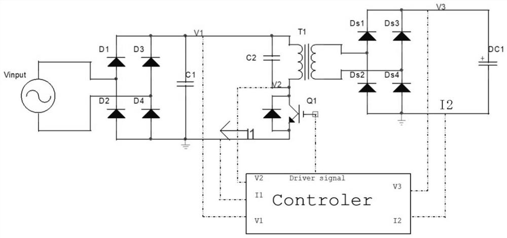
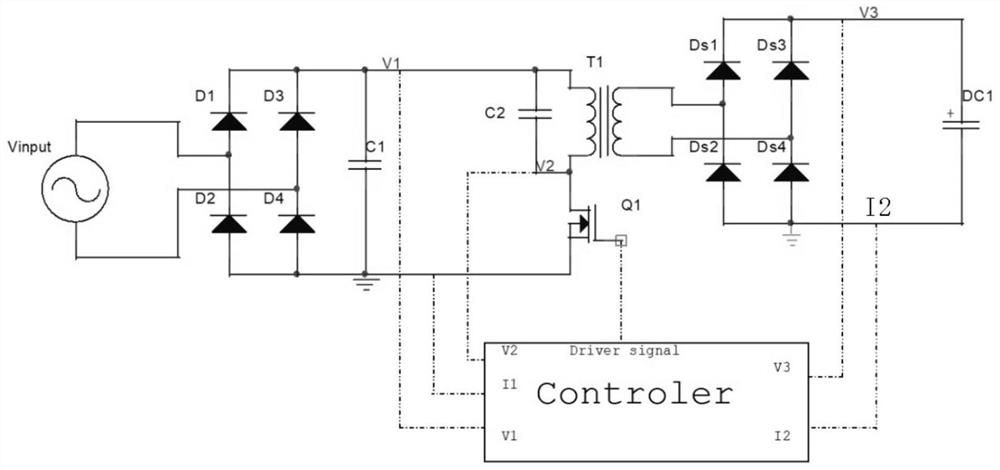
[0042] The working principle is as follows: if figure 2 As shown, the circuit is composed of diodes D1~D4 to form a primary side bridge rectifier unit, the output end of the primary side bridge rectifier unit is electrically connected to capacitor C1, and capacitor C1 is a high frequency capacitor, which mainly provides a high frequency circuit for the circuit; the primary side bridge The output terminal of the bridge type rectifier unit is connected to the air-gapped transformer T1 through the switch tube Q1 with an anti-parallel diode. The negative pole of T1 is connected to the negative pole of the output terminal of the primary bridge rectifier unit through the switch tube Q1, the input terminal of the transformer T1 is electrically connected to the resonant capacitor C2, and the output terminal of the transformer T1 is connected to the secondary bridge rectifier unit, wherein the secondary bridge rectifier unit Composed of diodes Ds1-Ds4, a DC filter capacitor DC1 is ele...
Embodiment 2
[0045] Replace the switching tube Q1 in Embodiment 1 with a MOS tube, so that its own body diode can be used to form a loop. Specific as image 3 shown.
Embodiment 3
[0047] In the case that the primary and secondary sides do not need to be isolated, the inductor L11 can be used to replace the transformer to form a typical boost circuit. In particular, the tap of the inductor is used to form a boost ratio, and a MOS tube with a relatively low withstand voltage can be selected. The Rdson is smaller, the conduction loss is lower, and the cost of the low-voltage MOS tube is also lower. The discharge principle of the battery is as follows: when the MOS transistor Q11 is turned on, the resonant circuit of the inductor L11 and C11 stores energy. When the MOS transistor Q11 is turned off, the inductor L11 generates a left-negative and right-positive voltage, which is a resonant voltage waveform. Reverse charging, when the voltage exceeds the output voltage V DC1When the diode D11 conducts to supplement energy to DC1, when the voltage on C11 is resonated back to the clamping voltage nV battery When (n is the transformation ratio of the inductance ...
PUM
 Abstract
Description
Claims
Application Information