Oxide thin film transistor with improved conductivity and liquid crystal display

A technology of oxide film and oxide conductor, applied in transistors, semiconductor devices, electric solid devices, etc., can solve the problem of uneven display, and achieve the effect of solving uneven display, improving conductivity, and high precision of graphics

Pending Publication Date: 2022-06-07
SHANTOU GOWORLD DISPLAY TECH CO LTD
View PDF0 Cites 0 Cited by
  • Summary
  • Abstract
  • Description
  • Claims
  • Application Information

AI Technical Summary

Problems solved by technology

[0007] The technical problem to be solved by the present invention is to provide an oxide thin film transistor and a liquid crystal display with improved conductivity. Stability, it can solve the problem of uneven display when applied to LCD monitors

Method used


Image

  • Oxide thin film transistor with improved conductivity and liquid crystal display
  • Oxide thin film transistor with improved conductivity and liquid crystal display
  • Oxide thin film transistor with improved conductivity and liquid crystal display

Examples


Embodiment 1

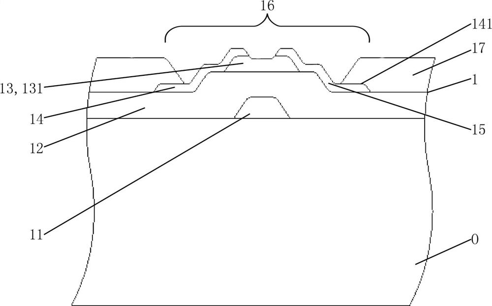
[0035] as Figure 1As shown, such an improved conductivity of the oxide thin film transistor 1, comprising a gate 11 and an insulating layer 12 disposed on the substrate 0, and an active layer 13, a source 14 and a drain 15, the gate 11 is covered by the insulating layer 12, the active layer 13, the source 14, the drain 15 are disposed on the upper surface of the insulating layer 12, the source 14, the drain 15 relatively set; The active layer 13 is an oxide semiconductor layer 131, the source 14, the drain 15 are patterned by the oxide conductor layer 141, the source 14, the drain 15 and the active layer 13 are superimposed to form a conductive channel 16; Oxide thin film transistor 1 further comprises a metal circuit 17, the metal circuit 17 is disposed on the insulation layer 12 and is located on the periphery of the oxide conductor layer 141, and the metal line 17 is connected to the source 14, the drain 15 is mated.

[0036] Active layer 13 is an oxide semiconductor layer 131,...

Embodiment 2

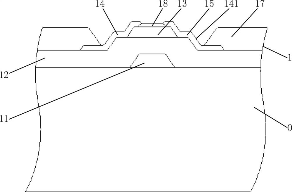
[0043] reference Figure 2 , in the case where other moieties are the same as Example I, the difference is that: in the present embodiment, the oxide thin film transistor 1 adopts a staggered channel etched structure, the source 14, the drain 15 portion is superimposed on top of the active layer 13; Oxide thin film transistor 1 further comprises a protective layer 18, the protective layer 18 is covered on the upper surface of the active layer 13 and is between the source 14 and the drain 15; The protective layer 18 is a polymer coating or an inorganic coating such as silicon oxide and silicon nitride.

Embodiment 3

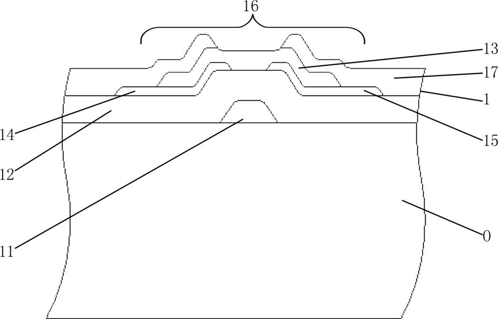
[0045] reference Figure 3 , in the case of other moieties are the same as Example I, the difference is that: in the present embodiment, the oxide thin film transistor 1 adopts a coplanar channel etched structure, the source 14, the drain 15 portion of the pad is located at the bottom of the active layer 13.


PUM

PropertyMeasurementUnit
thicknessaaaaaaaaaa
thicknessaaaaaaaaaa
thicknessaaaaaaaaaa

Abstract

The invention relates to an oxide thin film transistor with improved conductivity and a liquid crystal display, the oxide thin film transistor comprises a grid electrode, an insulating layer, an active layer, a source electrode and a drain electrode, the grid electrode and the insulating layer are arranged on a substrate, the grid electrode is covered by the insulating layer, the active layer, the source electrode and the drain electrode are arranged on the upper surface of the insulating layer, and the source electrode and the drain electrode are oppositely arranged. The thin film transistor is characterized in that the active layer is an oxide semiconductor layer, the source electrode and the drain electrode are formed by patterning an oxide conductor layer, and the source electrode, the drain electrode and the active layer are in lap joint to form a conductive channel. According to the invention, the conductivity can be effectively improved, the structure is stable and controllable, good stability after modification can be ensured, and when the liquid crystal display is applied, the problem of conductivity consistency of different TFT devices can be effectively solved, so that the problem of uneven display of the display is solved.

Description

Technical field [0001] The present invention relates to the field of liquid crystal display technology, specifically to an oxide thin film transistor and liquid crystal display that improves electrical conductivity. Background [0002] Oxide thin film transistors (also known as oxide TFT) are thin film transistors that use an oxide semiconductor layer as an active layer or channel. Due to the high electron mobility of oxide semiconductors and their better theoretical conductivity, this TFT device is suitable for high-resolution, high-refresh rate TFT displays with demanding charge and discharge control, as well as OLED displays and micro-LED displays based on current drive. [0003] At present, oxide thin film transistors generally adopt a bottom gate design with a gate pad at the bottom of the active layer, which can be further divided into staggered and coplanar designs. [0004] For the staggered design of the oxide thin film transistor, its source / drain is stacked on top of...

Claims


Application Information

Patent Timeline
Patent Type & Authority Applications(China)
IPC IPC(8): H01L29/786H01L29/10H01L27/12
CPCH01L29/7869H01L29/78696H01L29/1033H01L27/1225H01L27/124
Inventor 沈奕陈玉云杨秋强吕岳敏陈远明余荣
Owner SHANTOU GOWORLD DISPLAY TECH CO LTD
Why Eureka
Try Eureka