Silicon-based heterojunction solar cell structure and preparation method thereof

A solar cell and heterojunction technology, applied in circuits, electrical components, photovoltaic power generation, etc., can solve large parasitic absorption and series resistance, affect the short-circuit current and fill factor of heterojunction cells, and affect the improvement of heterojunction efficiency, etc. problem, to achieve low parasitic absorption, low reflection, and good passivation

Pending Publication Date: 2022-06-21
ZHEJIANG AIKO SOLAR ENERGY TECH CO LTD
View PDF0 Cites 0 Cited by
  • Summary
  • Abstract
  • Description
  • Claims
  • Application Information

AI Technical Summary

Problems solved by technology

There are some structural defects in the conventional heterojunction cell structure, which affect the efficiency improvement of the heterojunction. For example, in the common HIT cell structure, the usual structure is to set an amorphous silicon layer on the upper surface of the single crystal silicon wafer , set a transparent TCO thin film layer...

Method used


Image

  • Silicon-based heterojunction solar cell structure and preparation method thereof
  • Silicon-based heterojunction solar cell structure and preparation method thereof

Examples


Embodiment 1

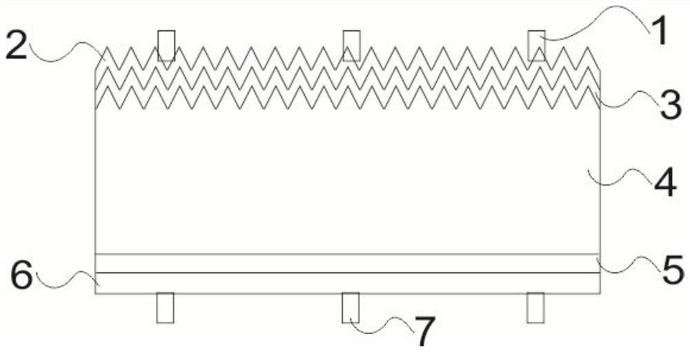
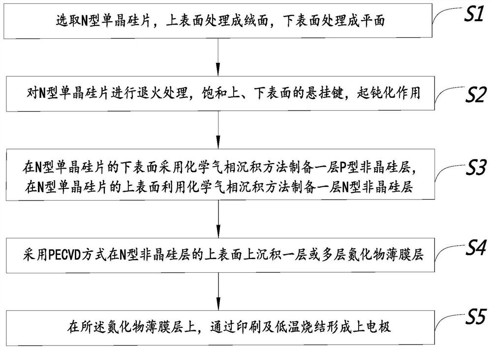
[0032] like figure 1 As shown, this embodiment discloses a silicon-based heterojunction solar cell structure, which includes an N-type single crystal silicon wafer 4 and an N-type amorphous silicon layer 3 located on the upper surface of the N-type single crystal silicon wafer 4 , a P-type amorphous silicon layer 5 located on the lower surface of the N-type single crystal silicon wafer 4, an upper electrode 1 is arranged above the N-type amorphous silicon layer 3, and a lower electrode is arranged below the P-type amorphous silicon layer 5 7. One or more layers of nitride thin film layers 2 are arranged between the upper electrode 1 and the N-type amorphous silicon layer 3 , and the nitride thin film layer 2 is deposited on the upper surface of the N-type amorphous silicon layer 3 .

[0033] First of all, because the traditional TCO transparent conductive film layer itself has shortcomings such as light transmittance and parasitic absorption, which reduces the short-circuit c...


PUM

PropertyMeasurementUnit
Thicknessaaaaaaaaaa
Widthaaaaaaaaaa
Depthaaaaaaaaaa

Abstract

The invention discloses a silicon-based heterojunction solar cell structure, which belongs to the field of solar cell structures and comprises an N-type monocrystalline silicon wafer, an N-type amorphous silicon layer positioned on the upper surface of the N-type monocrystalline silicon wafer and a P-type amorphous silicon layer positioned on the lower surface of the N-type monocrystalline silicon wafer, an upper electrode is arranged above the N-type amorphous silicon layer, and a lower electrode is arranged below the P-type amorphous silicon layer. One or more nitride thin film layers are arranged between the upper electrode and the N-type amorphous silicon layer, the nitride thin film layers are deposited on the upper surface of the N-type amorphous silicon layer, and a TCO transparent conductive thin film layer is arranged between the P-type amorphous silicon layer and the lower electrode. The invention further discloses a preparation method of the silicon-based heterojunction solar cell structure. The solar cell structure has the advantage that the short-circuit current of the solar cell structure can be improved.

Description

【Technical field】 [0001] The invention relates to a silicon-based heterojunction solar cell structure and a preparation method, and belongs to the field of solar cell structures. 【Background technique】 [0002] At present, heterojunction solar cells have not been able to achieve large-scale commercial applications due to factors such as high fabrication costs and narrow process technology windows. The conventional heterojunction cell structure has some structural defects, which affect the efficiency improvement of the heterojunction. For example, in the common HIT cell structure, the usual structure is to set an amorphous silicon layer on the upper surface of a single crystal silicon wafer. , a transparent TCO thin film layer is arranged on the amorphous silicon layer, but because the transparent TCO thin film layer itself has a certain light transmittance, this leads to the existence of a large parasitic absorption of the intrinsic amorphous silicon layer and the doped amor...

Claims


Application Information

Patent Timeline
IPC IPC(8): H01L31/0216H01L31/0747H01L31/20
CPCH01L31/02168H01L31/0747H01L31/202H01L31/208Y02E10/50
Inventor 常纪鹏王永谦张建军林纲正陈刚
Owner ZHEJIANG AIKO SOLAR ENERGY TECH CO LTD
Why Eureka
Try Eureka