Separation gate SiC MOSFET integrated with heterojunction diode and manufacturing method thereof

A diode and heterojunction technology, which is applied in the field of power semiconductor devices, can solve the problems of long forward turn-on voltage drop and reverse recovery time of parasitic body diodes, so as to improve the excessive forward turn-on voltage drop, reduce resistance, and improve switching speed effect

Active Publication Date: 2022-06-24
UNIV OF ELECTRONICS SCI & TECH OF CHINA
View PDF9 Cites 2 Cited by
  • Summary
  • Abstract
  • Description
  • Claims
  • Application Information

AI Technical Summary

Problems solved by technology

The present invention integrates a heterojunction diode in the three-dimensional y direction of the SiC MOSFET, which can effectively improve the excessive forward turn-on voltage drop and long reverse recovery time of the parasitic body diode without increasing the cell width of the SiC MOSFET. And other issues

Method used


Image

  • Separation gate SiC MOSFET integrated with heterojunction diode and manufacturing method thereof
  • Separation gate SiC MOSFET integrated with heterojunction diode and manufacturing method thereof
  • Separation gate SiC MOSFET integrated with heterojunction diode and manufacturing method thereof

Examples


Embodiment Construction

[0044] The principles and features of the present invention will be described below with reference to the accompanying drawings. The examples are only used to explain the present invention, but not to limit the scope of the present invention.

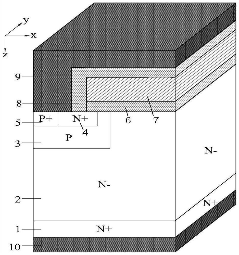
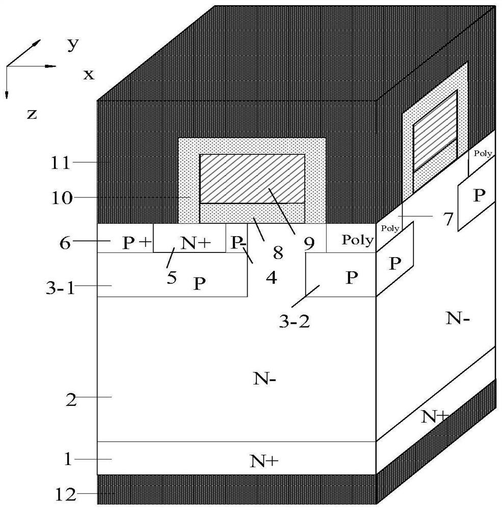
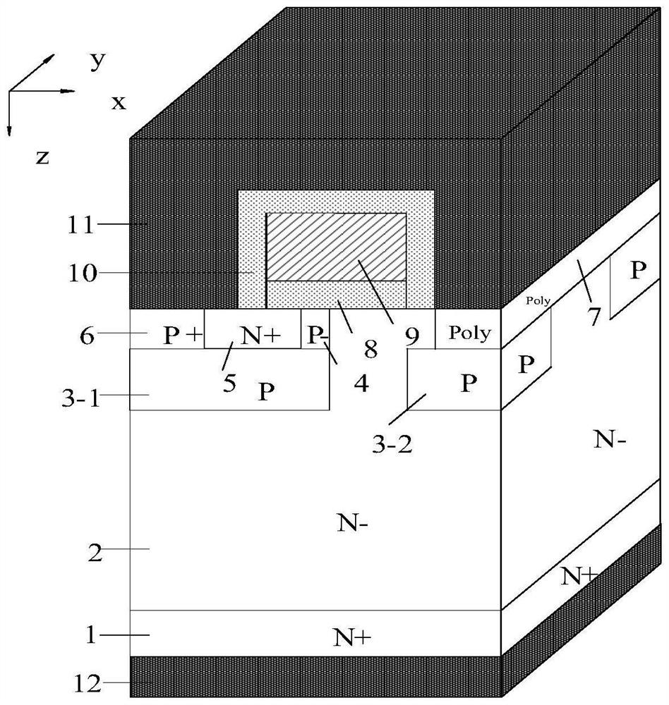
[0045] like figure 2 As shown, the first embodiment of the present invention provides a split-gate SiC MOSFET integrating heterojunction diodes, and the three-dimensional direction of the device is defined in a three-dimensional rectangular coordinate system: the lateral direction of the device is defined as the X-axis direction, and the vertical direction of the device is Y. The axial direction, the longitudinal direction of the device, that is, the third dimensional direction is the Z-axis direction. It is characterized in that its half-cell structure includes: along the Z-axis direction, the back drain metal 12, the N-type substrate layer 1 and the N-type substrate layer 1 and N-drift region 2; along the X-axis direction, the top si...


PUM


Abstract

The invention belongs to the technical field of power semiconductor devices, and relates to a separation gate SiCMOSFET of an integrated heterojunction diode and a manufacturing method of the separation gate SiCMOSFET. According to the invention, the heterojunction diode is integrated in the three-dimensional y direction of the SiC MOSFET, so that the cell width of the SiC MOSFET is not increased, the problems of overlarge forward turn-on voltage drop, overlong reverse recovery time and the like of a parasitic diode can be effectively solved, and compared with an internally integrated SBD, the integrated heterojunction diode has smaller forward voltage drop. According to the mode of integrating the heterojunction diode, the area of an active region does not need to be additionally increased, the integration level is higher, and the width of the JFET region is not increased. Meanwhile, the spaced P-type doped regions are introduced in the y direction of the JFET region, so that the electric field distribution of the JFET region of the device and the peak electric field in the oxide layer during blocking work can be improved, a CSL layer with higher concentration can be adopted during design, and the forward conduction characteristic of the device is improved and the resistance of the device during forward conduction is reduced while the reverse blocking characteristic of the device is not reduced.

Description

technical field [0001] The invention belongs to the technical field of power semiconductor devices, and in particular relates to a split gate SiC MOSFET integrated with a heterojunction diode and a manufacturing method thereof. Background technique [0002] Power semiconductor devices, as the core components in power electronic systems, have been an indispensable and important electronic component in production and life since their invention in the 1970s. The metal-oxide-semiconductor field-effect transistor (MOSFET) structure was developed in the mid-1970s, and the performance has been greatly improved compared to the bipolar transistor BJT. The main problem of the bipolar transistor structure is when high voltage applications are used. The current gain is low, and the power bipolar transistors cannot operate at high frequencies due to the longer charge storage time due to minority carrier injection in the drift region. In inductive load applications, the hard switching pr...

Claims


Application Information

Patent Timeline
Patent Type & Authority Applications(China)
IPC IPC(8): H01L29/06H01L29/78H01L21/336
CPCH01L29/0684H01L29/7804H01L29/66712Y02B70/10
Inventor 张金平吴庆霖陈伟张波
Owner UNIV OF ELECTRONICS SCI & TECH OF CHINA
Why Eureka
Try Eureka