Planar high electron mobility transistor

A high electron mobility, transistor technology, applied in circuits, electrical components, semiconductor devices, etc., can solve the problems of high specific on-resistance, non-uniformity of normally-off GaN HEMTs, etc., to reduce energy loss. Effect

Pending Publication Date: 2022-06-24
NANTONG SANRISE INTEGRATED CIRCUIT CO LTD
View PDF0 Cites 1 Cited by
  • Summary
  • Abstract
  • Description
  • Claims
  • Application Information

AI Technical Summary

Problems solved by technology

However, the industry does not have a uniform approach to realize normally-off GaN HEMTs
[0003] The specific on-resistance (Ron,sp) of existing power devices is related to the breakdown voltage (Breakdown Voltage). The higher the breakdown voltage, the higher the specific on-resistance will be.

Method used


Image

  • Planar high electron mobility transistor
  • Planar high electron mobility transistor
  • Planar high electron mobility transistor

Examples


Embodiment Construction

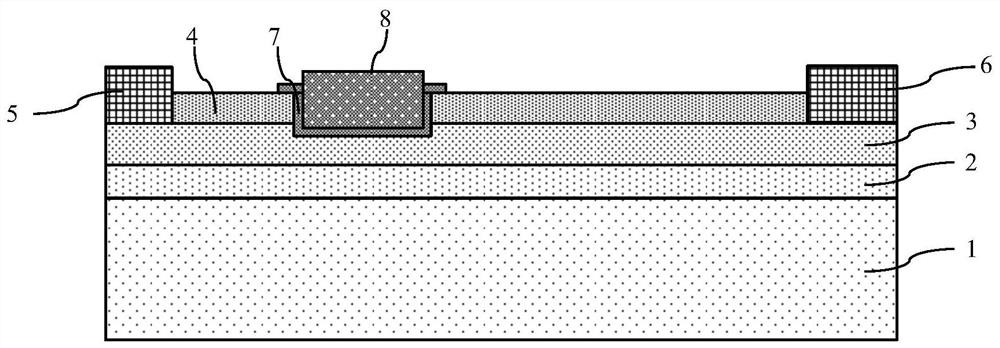
[0062] The first embodiment of the present invention is a planar high electron mobility transistor:

[0063] like figure 1 As shown, it is a schematic structural diagram of the planar high electron mobility transistor according to the first embodiment of the present invention; the device unit of the planar high electron mobility transistor according to the first embodiment of the present invention includes:

[0064] The first semiconductor epitaxial layer 3 and the second semiconductor epitaxial layer 4 formed on the surface of the first semiconductor epitaxial layer 3, the first semiconductor epitaxial layer 3 and the second semiconductor epitaxial layer 4 form a first heterojunction and are A two-dimensional electron gas is formed at the first heterojunction interface.

[0065] The trench gate includes a gate trench, a gate dielectric layer 7 formed on the inner surface of the gate trench, and a gate conductive material layer 8 filling the gate trench.

[0066] The gate tr...


PUM

PropertyMeasurementUnit
thicknessaaaaaaaaaa
strengthaaaaaaaaaa

Abstract

The invention discloses a planar high-electron-mobility transistor which comprises a heterojunction composed of a first semiconductor epitaxial layer and a second semiconductor epitaxial layer and two-dimensional electron gas located at the interface of the heterojunction. The bottom surface of the gate trench of the trench gate is located at the bottom of the two-dimensional electron gas to cut off the two-dimensional electron gas; when the gate-source voltage is greater than or equal to the threshold voltage, an inversion layer is formed on the surface of the first semiconductor epitaxial layer covered by the side surface and the bottom surface of the gate conductive material layer, and two-dimensional electron gas at the source-drain end is conducted so that the device is conducted; and when the gate-source voltage is smaller than the threshold voltage, the source-drain end two-dimensional electron gas is disconnected and the device is closed. According to the invention, the trench gate of the MOSFET is adopted to control the conduction channel of the HEMTs, so that the threshold voltage can be conveniently and independently adjusted, and the normally-closed planar high-electron-mobility transistor can be conveniently realized; and the electric field of the drift region can be conveniently adjusted, so that the electric field of the drift region is uniformly distributed, the breakdown voltage of the device can be improved, and the specific on-resistance and size are reduced.

Description

technical field [0001] The present invention relates to the field of semiconductor integrated circuit manufacturing, in particular to a planar high electron mobility transistor (HEMTs). Background technique [0002] As a typical wide-bandgap semiconductor material, gallium nitride is often used in the fabrication of power semiconductor devices in various researches. Especially in the application of high temperature and high pressure, gallium nitride material has more obvious advantages due to its large forbidden band width of 3.4eV, high breakdown electric field strength of 3MV / cm, high electron mobility and high thermal conductivity. So far, the mainstream devices of gallium nitride are still focused on the research of planar HEMTs. The manufacturing process of such devices has gradually matured and has entered the stage of marketization. However, there is no consensus in the industry on how to implement normally-off GaN HEMTs. [0003] The specific on-resistance (Ron, sp...

Claims


Application Information

Patent Timeline
Patent Type & Authority Applications(China)
IPC IPC(8): H01L29/778H01L29/423H01L29/06H01L21/335
CPCH01L29/4236H01L29/0615H01L29/7787H01L29/66462H01L29/2003H01L29/7786H01L29/0657H01L29/7783H01L29/4175H01L29/205
Inventor 周翔
Owner NANTONG SANRISE INTEGRATED CIRCUIT CO LTD
Why Eureka
Try Eureka