Semiconductor memory structure and manufacturing method thereof

A semiconductor and memory technology, applied in semiconductor/solid-state device manufacturing, transistors, electrical components, etc., can solve the problems that holes cannot be completely eliminated, the process is complicated, and it is difficult to produce on a large scale, so as to achieve stable work, reduced resistance, and leakage The effect of problem mitigation

Pending Publication Date: 2022-07-01
INST OF MICROELECTRONICS CHINESE ACAD OF SCI +1
View PDF0 Cites 0 Cited by
  • Summary
  • Abstract
  • Description
  • Claims
  • Application Information

AI Technical Summary

Problems solved by technology

[0007] However, repeated deposition and etching by the above method can neither completely eliminate t

Method used


Image

  • Semiconductor memory structure and manufacturing method thereof
  • Semiconductor memory structure and manufacturing method thereof
  • Semiconductor memory structure and manufacturing method thereof

Examples


Example Embodiment

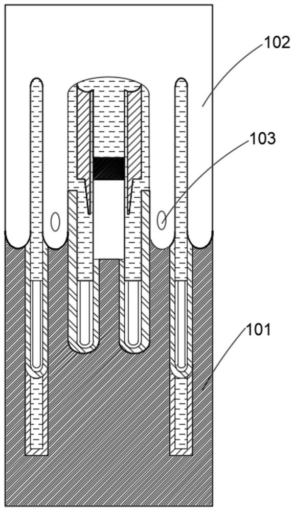
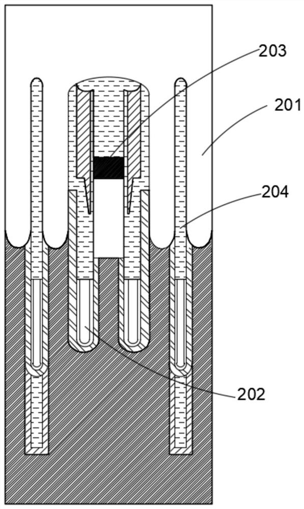
[0030] Hereinafter, embodiments of the present disclosure will be described with reference to the accompanying drawings. It should be understood, however, that these descriptions are exemplary only, and are not intended to limit the scope of the present disclosure. Also, in the following description, descriptions of well-known structures and techniques are omitted to avoid unnecessarily obscuring the concepts of the present disclosure.

[0031] Various structural schematic diagrams according to embodiments of the present disclosure are shown in the accompanying drawings. The figures are not to scale, some details have been exaggerated for clarity, and some details may have been omitted. The shapes of the various regions and layers shown in the figures, as well as their relative sizes and positional relationships are only exemplary, and in practice, there may be deviations due to manufacturing tolerances or technical limitations, and those skilled in the art should Regions / la...


PUM


Abstract

The invention relates to a semiconductor memory structure and a manufacturing method thereof. The semiconductor structure comprises a semiconductor substrate, and the semiconductor substrate comprises an active region; the dielectric layer is positioned on the active region; the contact hole is located in the dielectric layer, and a part of the active region is exposed out of the contact hole; the contact hole is filled with a conducting medium; and the conducting medium is selective epitaxial growth silicon. The manufacturing method comprises the following steps: providing a semiconductor substrate, and forming an active region in the semiconductor substrate; forming a dielectric layer above the semiconductor substrate, and forming a contact hole exposing a part of the active region in the dielectric layer; and selectively and epitaxially growing a silicon layer in the contact hole. Selective epitaxial growth (SEG) silicon is adopted, and almost no hole exists, so that the resistance is smaller, and the electrical characteristic is more excellent.

Description

technical field [0001] The present invention relates to the field of semiconductors, in particular to a semiconductor memory structure and a manufacturing method thereof. Background technique [0002] In a semiconductor manufacturing process, an etching process is used to form a contact hole in a dielectric layer, and then a conductive material is deposited in the contact hole for electrical connection between semiconductor devices, which is a widely used process. The contact holes can be directly electrically connected to the gate, source and drain of the device, and can also be used for electrical connection between layers. Wire connections in many semiconductor devices are critical, and the technical application of connecting wires is becoming increasingly difficult. [0003] Take DRAM as an example, such as figure 1 As shown, most of the wires buried in the contact holes in the active area unit 101 connected to the capacitor are made of polysilicon 102. With the develo...

Claims


Application Information

Patent Timeline
IPC IPC(8): H01L27/108H01L21/8242
CPCH10B12/34H10B12/03
Inventor 崔基雄白国斌高建峰王桂磊田光辉丁云凌
Owner INST OF MICROELECTRONICS CHINESE ACAD OF SCI
Why Eureka
Try Eureka