Supercharge Your Innovation With Domain-Expert AI Agents!

Epitaxial structure of semiconductor device, preparation method of epitaxial structure and semiconductor device

An epitaxial structure, semiconductor technology, applied in the fields of semiconductor/solid-state device manufacturing, semiconductor devices, electrical components, etc., can solve the problems of two-dimensional electron gas electron mobility reduction, resistivity reduction, device performance impact, etc., to ensure electron migration. rate, the effect of increasing the resistivity

Pending Publication Date: 2022-07-01
DYNAX SEMICON
View PDF0 Cites 0 Cited by
  • Summary
  • Abstract
  • Description
  • Claims
  • Application Information

AI Technical Summary

Problems solved by technology

The second method is to perform ion implantation in the buffer layer to form a high-resistivity region. This method can alleviate the drain hysteresis effect, but when the concentration of implanted ions is insufficient, the resistivity will decrease, and when the concentration of implanted ions is high, it will It leads to the decrease of electron mobility in the two-dimensional electron gas, which in turn affects the performance of the device

Method used


Image

  • Epitaxial structure of semiconductor device, preparation method of epitaxial structure and semiconductor device
  • Epitaxial structure of semiconductor device, preparation method of epitaxial structure and semiconductor device
  • Epitaxial structure of semiconductor device, preparation method of epitaxial structure and semiconductor device

Examples


Embodiment Construction

[0037] The present invention will be further described in detail below in conjunction with the accompanying drawings and embodiments. It should be understood that the specific embodiments described herein are only used to explain the present invention, but not to limit the present invention. In addition, it should be noted that, for the convenience of description, the drawings only show some but not all structures related to the present invention.

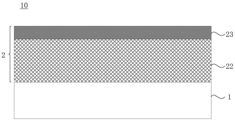
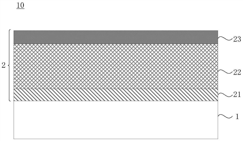
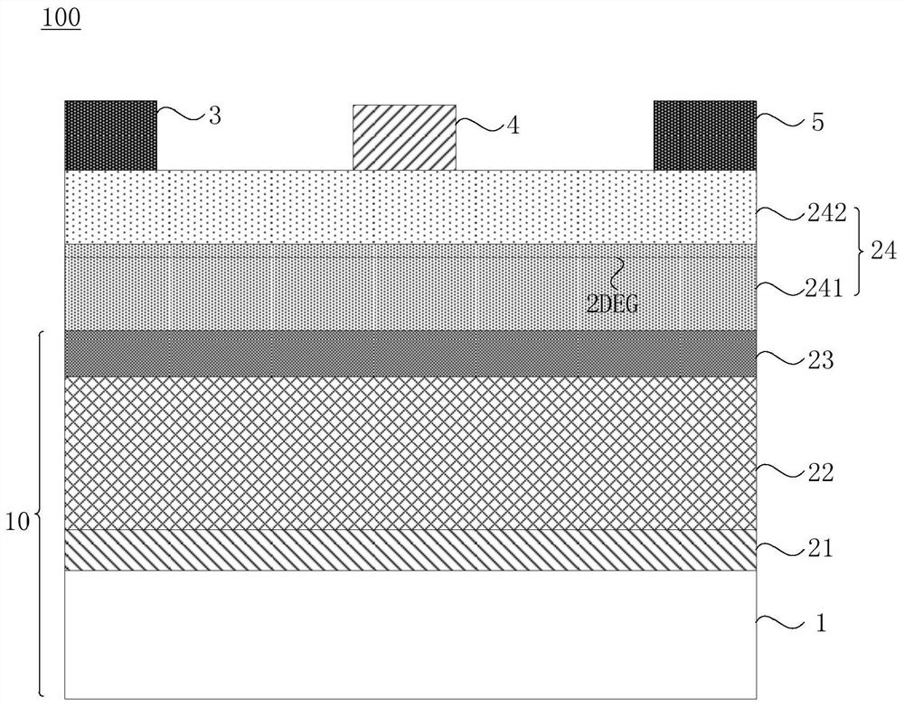
[0038] figure 1 is a schematic structural diagram of an epitaxial structure of a semiconductor device provided by an embodiment of the present invention, see figure 1 , an epitaxial structure 10 of a semiconductor device includes a substrate 1 and a semiconductor layer 2 on one side of the substrate 1 . The semiconductor layer 2 at least includes a buffer layer 22 and a barrier layer 23 stacked on one side of the substrate 1; the forbidden band width of the barrier layer 23 is larger than that of the buffer layer 22, and at least...


PUM

PropertyMeasurementUnit
Resistivityaaaaaaaaaa

Abstract

The embodiment of the invention discloses an epitaxial structure of a semiconductor device, a preparation method of the epitaxial structure and the semiconductor device. The epitaxial structure comprises a substrate and a semiconductor layer located on one side of the substrate. The semiconductor layer at least comprises a buffer layer and a barrier layer which are stacked on one side of the substrate; the forbidden bandwidth of the barrier layer is larger than that of the buffer layer, ions are at least injected into the buffer layer and the barrier layer, and the injection concentration of the ions in the barrier layer is smaller than that of the ions in the buffer layer. The semiconductor device using the epitaxial structure can ensure the electron mobility while reducing electric leakage.

Description

technical field [0001] Embodiments of the present invention relate to the technical field of semiconductors, and in particular, to an epitaxial structure of a semiconductor device, a preparation method thereof, and a semiconductor device. Background technique [0002] The semiconductor material gallium nitride has become a research hotspot in the semiconductor field due to its large band gap, high electron saturation drift velocity, high breakdown field strength, and good thermal conductivity. For example, it is used to fabricate gallium nitride high electron mobility transistors. (GaN HEMT) devices. [0003] Since gallium nitride crystals usually contain N-type impurities, the resistivity of the buffer layer is low, and the leakage of semiconductor devices cannot be effectively controlled. To solve this problem, there are two main implementation methods in the prior art: one method is to neutralize N-type impurities by doping impurities during epitaxial growth, but this me...

Claims


Application Information

Patent Timeline
IPC IPC(8): H01L29/06H01L29/20H01L21/335H01L29/778
CPCH01L29/0684H01L29/2003H01L29/66462H01L29/778
Inventor 钱洪途裴轶张晖
Owner DYNAX SEMICON
Features
  • R&D
  • Intellectual Property
  • Life Sciences
  • Materials
  • Tech Scout
  • Unparalleled Data Quality
  • Higher Quality Content
  • 60% Fewer Hallucinations
Learn More