Eureka AIR delivers breakthrough ideas for toughest innovation challenges, trusted by R&D personnel around the world.

High-power diode structure and manufacturing method

A technology of high-power diodes and manufacturing methods, applied in the field of diodes, can solve problems such as large thermal resistance of diodes, difficulty in picking up and positioning, poor concentricity and poor consistency of components, achieve enhanced temperature shock resistance, reduce assembly and positioning difficulties, Effect of improving thermal fatigue resistance

Pending Publication Date: 2022-07-08
CHINA ZHENHUA GRP YONGGUANG ELECTRONICS CO LTD STATE OWNED NO 873 FACTORY
View PDF0 Cites 0 Cited by
  • Summary
  • Abstract
  • Description
  • Claims
  • Application Information

AI Technical Summary

Problems solved by technology

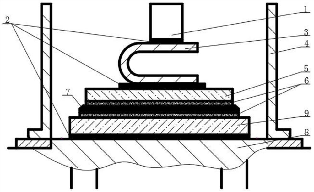
[0003] 1. The thermal fatigue resistance of lead-tin-silver solder is poor, the welding stress between the chip and the electrode is large, the fatigue resistance of the diode is only about 2,000 times, and the service life is short
[0004] 2. The melting point of lead-tin-silver solder is more than 200 degrees, and the high temperature work is limited
[0005] 3. The traditional diode core and base are soldered with lead-tin-silver solder, which is thicker and has poor wetting with the chip, resulting in a large thermal resistance of the diode, often exceeding 2°C / W. The greater the thermal resistance, the more heat generated by the chip. It is not easy to spread out, and the small power dissipation will reach the maximum allowable junction temperature of the diode, which is not conducive to the improvement of the power of the diode
[0006] 4. Lead-tin-silver solder is light and thin, difficult to pick up and locate, and difficult to assemble, so the production efficiency is low, and the concentricity and consistency of components are poor

Method used


Image

  • High-power diode structure and manufacturing method
  • High-power diode structure and manufacturing method
  • High-power diode structure and manufacturing method

Examples


Embodiment Construction

[0048] The technical solutions of the present invention are further described below, but the claimed scope is not limited to the description.

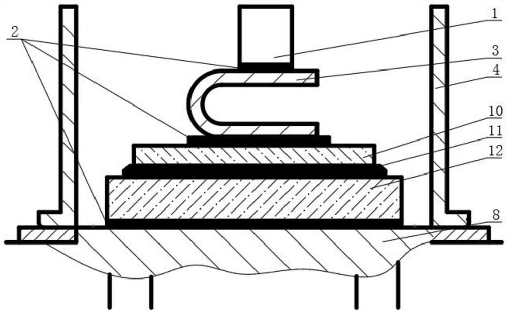
[0049] like Figure 1-2 shown:

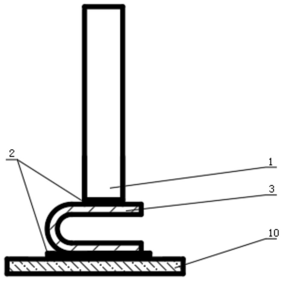
[0050] The present invention provides a high-power diode structure, comprising a base 8, a tube shell 4, and a double-sided vaporized aluminum chip 11, the tube shell 4 is mounted on the base 8, and the double-sided vaporized aluminum chip 11 is arranged in the tube shell 4; The bottom of the double-sided vaporized aluminum chip 11 is connected with a nickel-plated molybdenum sheet 12 below, and the bottom of the nickel-plated molybdenum sheet 12 is connected to the base 8; A buffer sheet 3 is connected to the top of the nickel-molybdenum-plated sheet 10 , and the inner lead 1 is connected to the top of the buffer sheet 3 .

[0051] By adopting the invention, the thermal fatigue resistance of the diode is greatly improved, from 2,000 times to more than 20,000 times, and it can work at a higher tempera...


PUM

PropertyMeasurementUnit
Groove depthaaaaaaaaaa

Abstract

The invention provides a high-power diode structure and a manufacturing method, the structure comprises a base, a tube shell and a double-sided aluminum evaporation chip, the tube shell is installed on the base, and the double-sided aluminum evaporation chip is arranged in the tube shell; the lower surface of the double-sided aluminum evaporation chip is connected with a lower nickel-plated molybdenum sheet, and the lower surface of the lower nickel-plated molybdenum sheet is connected with the base through a silver-copper soldering lug; the upper nickel-plated molybdenum sheet is connected to the upper surface of the double-sided aluminum evaporation chip, the buffer sheet is connected to the upper surface of the upper nickel-plated molybdenum sheet, and the inner lead is connected to the upper surface of the buffer sheet through the silver-copper soldering lug. According to the invention, the thermal fatigue resistance of the diode is greatly improved from 2,000 times to more than 20,000 times, and the diode can work at a higher temperature.

Description

technical field [0001] The present invention relates to the technical field of diodes, in particular to a high-power diode structure and a manufacturing method. Background technique [0002] At present, high-power diodes are usually used figure 1 Structure: the two sides of the double-sided nickel-plated chip are connected with double-sided nickel-plated sheets through lead, tin, and silver solder tabs. Lead wire; the double-sided nickel-plated sheet on the reverse side is connected to the base via a silver-copper solder tab. The structure has the following problems: [0003] 1. The lead-tin-silver solder has poor thermal fatigue resistance, and the welding stress between the chip and the electrode is large. The anti-fatigue performance of the diode is only about 2,000 times, and the service life is short. [0004] 2. The melting point of lead-tin-silver solder is more than 200 degrees, and high temperature work is limited. [0005] 3. The traditional diode die and base ...

Claims


Application Information

Patent Timeline
IPC IPC(8): H01L29/861H01L21/329H01L21/48H01L23/49H01L23/495
CPCH01L23/49548H01L23/49565H01L23/49H01L29/6609H01L29/861H01L21/4821
Inventor 张丽刘德军周嵘肖摇
Owner CHINA ZHENHUA GRP YONGGUANG ELECTRONICS CO LTD STATE OWNED NO 873 FACTORY
Why Eureka
Eureka Blog
Learn More