
Board-level system-level packaging method and packaging structure

A system-level packaging and board-level technology, which is applied to components of TV systems, manufacturing microstructure devices, and processing microstructure devices, etc., to achieve the effects of high packaging efficiency, improved packaging efficiency, and simple process flow

Inactive Publication Date: 2022-07-29
NINGBO SEMICON INT CORP
View PDF0 Cites 0 Cited by
  • Summary
  • Abstract
  • Description
  • Claims
  • Application Information

AI Technical Summary

Problems solved by technology

[0004] However, the existing system-in-package process still has great challenges

Method used


Image

  • Board-level system-level packaging method and packaging structure
  • Board-level system-level packaging method and packaging structure
  • Board-level system-level packaging method and packaging structure

Examples


Embodiment Construction

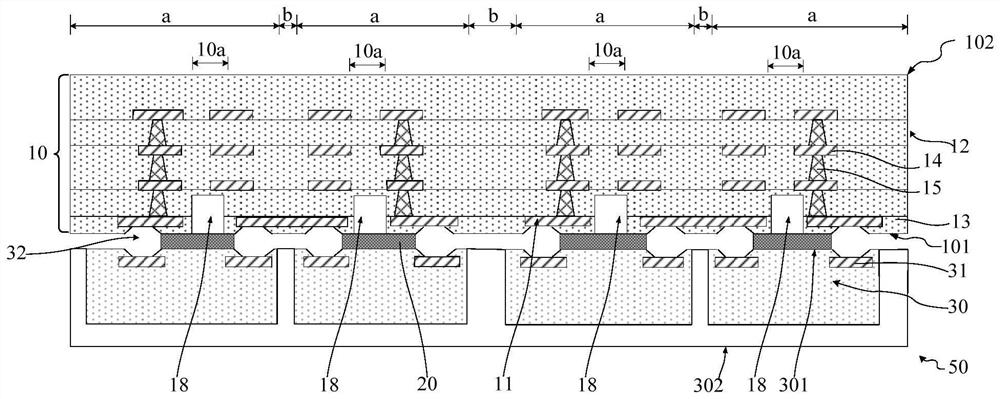
[0016] Existing system-in-package approaches still have great challenges. Specifically, taking flip-chip as an example, the existing system-level packaging method has the following disadvantages: 1. The process is complicated, resulting in low packaging efficiency; 2. Each chip needs to be soldered on the solder balls in sequence, and the packaging efficiency is low; 3. . It is necessary to use the welding process to realize the electrical connection between the chip and the circuit board, which is not compatible with the process in the front part of the packaging; 4. When a large pressure is accidentally applied during the process of dipping the flux, it is easy to cause the circuit board to crack.

[0017] In order to solve the technical problem, an embodiment of the present invention provides a board-level system-in-package method, including: providing a circuit board including a first surface and a second surface opposite to each other, the circuit board including a bonding...


PUM

PropertyMeasurementUnit
thicknessaaaaaaaaaa
heightaaaaaaaaaa
areaaaaaaaaaaa

Abstract

The invention discloses a board-level system-level packaging method and a packaging structure, and the method comprises the steps: bonding a first device wafer on a first surface, enabling a first chip to be located above a cavity, and enabling a first welding pad and a second welding pad to form a first gap in an opposite manner; forming a first conductive bump in the first gap through an electroplating process, wherein the first conductive bump is electrically connected with the first welding pad and the second welding pad; and after the first conductive bumps are formed, cutting the circuit board from one side of the second surface along the cutting area to form a cutting groove penetrating through the circuit board. According to the invention, the packaging efficiency of a board-level system-level packaging process and the compatibility with a front chip forming process are improved.

Description

technical field [0001] Embodiments of the present invention relate to the field of semiconductor device manufacturing, and in particular, to a board-level system-level packaging method and packaging structure. Background technique [0002] System-in-package uses any combination to combine multiple active components / devices, passive components / devices, MEMS devices, discrete KGD (Known Good Die, known good chips) with different functions and prepared by different processes, such as optoelectronic chips , biochips, etc., are integrated and assembled in three dimensions (X direction, Y direction and Z direction) into a single standard package with a multi-layer device structure and can provide multiple functions to form a system or subsystem. [0003] Flip-chip (FC, Flip-Chip) soldering is a commonly used system-in-package method at present. The system-in-package method includes: providing a PCB circuit board, wherein solder balls arranged according to certain requirements are...

Claims


Application Information

Patent Timeline
Patent Type & Authority Applications(China)
IPC IPC(8): H01L21/60H01L21/78B81B7/00B81B7/02B81C1/00B81C3/00H05K1/18H05K3/34
CPCH01L24/83H01L24/81H01L24/11H01L24/97H01L24/32B81C1/00095B81C1/00261B81C3/001B81B7/02B81B7/0032B81B7/0006B81C1/00888H05K1/181H05K3/3436H01L2224/32238H01L2224/11462H05K2201/037H01L2224/96H01L2224/16225
Inventor 黄河向阳辉刘孟彬
Owner NINGBO SEMICON INT CORP
Learn More