Functional chip for 3D chip

A chip and functional technology, applied in the field of functional chips, can solve the problems of large resistance parasitic parameters and capacitance parasitic parameters, long manufacturing cycle, large chip area, etc., to reduce resistance parasitic parameters and capacitance parasitic parameters, reduce production costs, The effect of reducing the area

Pending Publication Date: 2022-07-29
XI AN UNIIC SEMICON CO LTD
View PDF0 Cites 0 Cited by
  • Summary
  • Abstract
  • Description
  • Claims
  • Application Information

AI Technical Summary

Problems solved by technology

At the same time, the diameter and length of the through-silicon vias are large, resulting in a very large chip area occupied by the through-silicon vias, large resistance parasitic parameters and capacitance parasitic parameters, long manufacturing cycle, and high cost.

Method used


Image

  • Functional chip for 3D chip
  • Functional chip for 3D chip
  • Functional chip for 3D chip

Examples


specific Embodiment 1

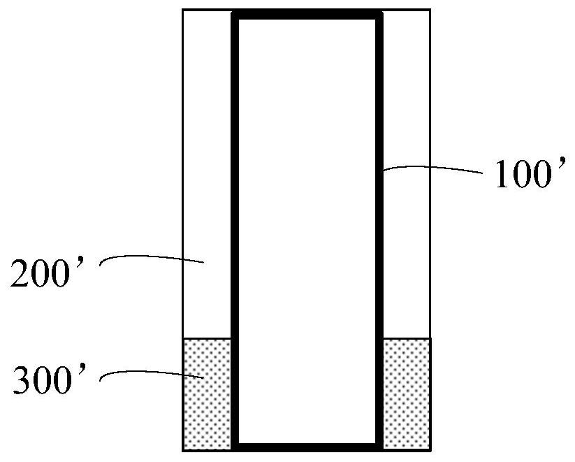
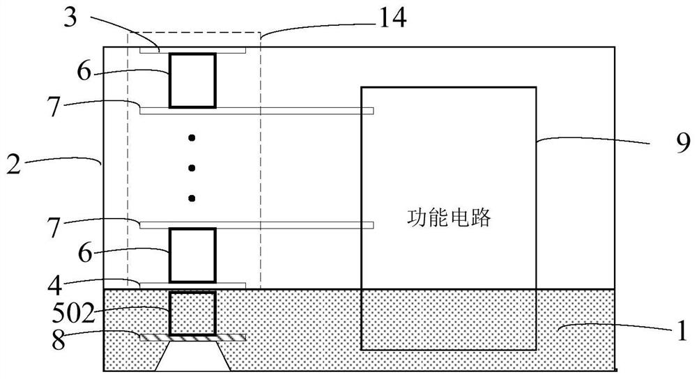
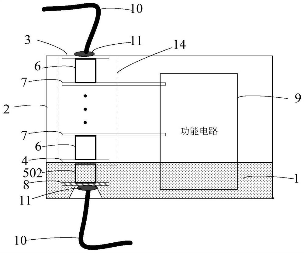
[0161] like figure 2 and image 3 As shown, an embodiment of the present invention provides a functional chip for a 3D chip, including: a substrate layer 1, a metal layer 2, a metal layer through hole component 14, a substrate through hole 5, a substrate conductor member 8, and functional circuit 9.

[0162] The metal layer through-hole component 14 includes: a first conductor part 3 , a second conductor part 4 , a conductor connection hole 6 and an on-chip conductor part 7 .

[0163] Wherein, the metal layer 2 includes a first surface and a second surface arranged opposite to each other, the second surface of the metal layer 2 is arranged on the substrate layer 1; the first conductor part 3 is formed on the first surface of the metal layer 2; the second conductor part 4 is formed on the second surface of the metal layer 2; the substrate through hole 5 is opened on the substrate layer 1, and is connected to the second conductor part 4 of the metal layer 2; the conductor con...

specific Embodiment 2

[0178] like figure 2 and image 3 As shown, on the basis of the specific embodiment 1, improvements or expansions can be made in the conductor connection holes 6 .

[0179] Since the conductor connection holes 6 are usually metal in-chip of a chip and through holes thereof, the conductor connection holes 6 can be connected to the internal circuit as the functional circuit 9 .

[0180] E.g, Figure 4 The functional circuit 9 can process 3D signals (passing through the chip) by connecting certain functional units through metal wires in the chip.

[0181] Functional units can act in the following ways:

[0182] 1. The switching circuit can be added to increase the choice;

[0183] 2. The drive function module can be added;

[0184] 3. The parallel-serial (serial-parallel) conversion function can be added;

[0185] 4. The function of computing with internal signals can be added.

[0186] For switching circuits:

[0187] The core idea of ​​the switching circuit is that the...


PUM


Abstract

The embodiment of the invention provides a functional chip for a 3D chip. The functional chip comprises a substrate layer; the metal layer comprises a first surface and a second surface which are oppositely arranged, and the second surface of the metal layer is arranged on the substrate layer; the metal layer perforation assembly is arranged in the metal layer, the metal layer perforation assembly comprises a first conductor piece, a second conductor piece and a conductor connecting hole, the first conductor piece is formed on the first surface of the metal layer, the second conductor piece is formed on the second surface of the metal layer, and the conductor connecting hole is formed in the metal layer; the second conductor piece is connected to the first conductor piece through the conductor connecting hole; the substrate through hole is formed in the substrate layer; and the functional circuit is connected to at least one of the first conductor piece and the second conductor piece. According to the functional chip, the etching process difficulty is reduced, the occupied area of the metal layer is reduced, the resistance parasitic parameter and the capacitance parasitic parameter are reduced, the preparation period of the functional chip is shortened, and the production cost is reduced.

Description

technical field [0001] The present invention relates to the technical field of semiconductors, and in particular, to a functional chip for 3D chips. Background technique [0002] With the development of chip technology and the increasing demand for information technology, 3D chips are increasingly appearing in the integrated circuit industry. The 3D chip may include a plurality of functional chips arranged in a stack. Due to the needs of signal transmission, the signal connection lines in the 3D chip need to pass through the functional chips constituting the 3D chip. The connection of the signal line from the front to the back of the chip is realized through the entire chip through the through hole, and the TSV (Through Silicon Via) process is mainly used at present. [0003] Since TSVs need to penetrate the entire chip, TSVs not only need to penetrate various materials that make up the stacked circuit, but also need to penetrate a very thick silicon substrate. Etching tec...

Claims


Application Information

Patent Timeline
Patent Type & Authority Applications(China)
IPC IPC(8): H01L23/498H01L23/367H01L23/373
CPCH01L23/49827H01L23/49811H01L23/49838H01L23/3672H01L23/3736H01L2224/48463H01L2224/4918
Inventor 李晓骏
Owner XI AN UNIIC SEMICON CO LTD
Why Eureka
Try Eureka