Multilayer structure current collector and preparation method thereof
A multi-layer structure, current collector technology, applied in the direction of electrode carrier/current collector, etc., can solve the problem of multi-layer structure current collector tensile strength and elongation attenuation, polymer film layer mechanical properties attenuation, reducing metal coating flow area and other problems, to achieve high mechanical properties and chemical stability, ensure battery performance, and reduce the number of evaporations.
- Summary
- Abstract
- Description
- Claims
- Application Information
AI Technical Summary
Problems solved by technology
Method used
Image
Examples
Embodiment
[0043] The present disclosure is more specifically described by the following examples, which are intended to be illustrative only, since various modifications and changes within the scope of the present disclosure will be apparent to those skilled in the art. Unless otherwise stated, all parts, percentages, and ratios reported in the following examples are on a weight basis, and all reagents used in the examples are either commercially available or synthesized according to conventional methods, and can be directly Used without further processing, and the instruments used in the examples are commercially available.
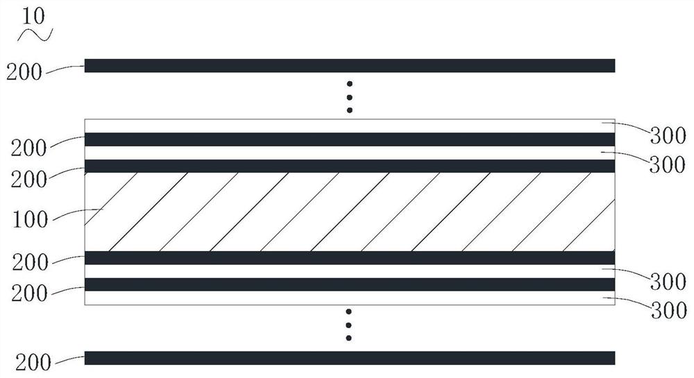
[0044] An embodiment of the present application also provides a method for preparing the multi-layer structure current collector 10 as described above, including the following steps:
[0045] Step 1: Select a 6 μm polymer film layer 100, a metal aluminum layer with a purity of 99.9%, and a graphite with a purity of 99.9%. The polymer film layer 100 is made of pol...
Embodiment 2
[0052] The difference between this embodiment and Embodiment 1 is that the thickness of the polymer film layer 100 is 25 μm. The metal aluminum layer is one layer, and the graphite layer is two layers. That is, in this embodiment, the thickness of the metal plating layer 300 is 500 nm. The thickness of the carbon coating 200 is 1000 nm. Finally, the multilayer structure current collector 10 of 30 μm was produced. In this embodiment, only the polymer thin film layer 100 needs to be continuously evaporated 6 times, and the metal plating layer 300 needs to be evaporated twice.
Embodiment 3
[0054] The difference between this embodiment and Embodiment 1 is that the thickness of the polymer film layer 100 is 1 μm. The metal aluminum layer is 5 layers, and the graphite layer is 6 layers. That is, in this embodiment, the thickness of the metal plating layer 300 is 32 nm. The thickness of the carbon coating 200 is 140 nm. Finally, the multilayer structure current collector 10 of 3 μm was produced.
PUM
| Property | Measurement | Unit |
|---|---|---|
| thickness | aaaaa | aaaaa |
| thickness | aaaaa | aaaaa |
| thickness | aaaaa | aaaaa |
Abstract
Description
Claims
Application Information


