Unlock instant, AI-driven research and patent intelligence for your innovation.

Gate drawing end clamping structure of planar power MOSFET (Metal-Oxide-Semiconductor Field Effect Transistor) device

A planar, high-power technology, applied in the direction of semiconductor devices, electrical components, circuits, etc., can solve problems such as insufficient, reverse collapse voltage influence, etc., to improve the ability of avalanche withstand current and avalanche withstand voltage, high withstand voltage, and ensure reliability The effect of resistance and pressure resistance

Active Publication Date: 2022-08-02
南京融芯微电子有限公司
View PDF7 Cites 1 Cited by
  • Summary
  • Abstract
  • Description
  • Claims
  • Application Information

AI Technical Summary

Problems solved by technology

However, because the diode structure is made of a whole piece of polysilicon in the terminal area of ​​the component to connect the gate drain, the reverse breakdown voltage of the component will be affected and insufficient, so it can only be used for low-to-medium voltage MOSFET components.

Method used


Image

  • Gate drawing end clamping structure of planar power MOSFET (Metal-Oxide-Semiconductor Field Effect Transistor) device
  • Gate drawing end clamping structure of planar power MOSFET (Metal-Oxide-Semiconductor Field Effect Transistor) device
  • Gate drawing end clamping structure of planar power MOSFET (Metal-Oxide-Semiconductor Field Effect Transistor) device

Examples


Embodiment 1

[0034] like Figure 9 As shown, a planar power MOSFET device with a gate-drain clamping structure, comprising:

[0035] N-type epitaxial layer 1, a first P-well region 2 and a second P-well region 5 are formed in the N-type epitaxial layer 1, and the first P-well region 2 and the second P-well region 5 are integrally connected, wherein , the first P-well region 2 is located in the terminal region, the second P-well region 5 is located in the active region, the distribution material of the first P-well region 2 is boron, and the overall concentration of boron is 10 13 cm -2 level, the distribution material of the second P-well region 5 is boron, and the overall concentration of boron is 10 15 cm -2 grade;

[0036] Field oxide layer 3, the field oxide layer 3 is located on the upper surface of the N-type epitaxial layer 1 in the terminal region, and the thickness of the field oxide layer 3 is 1.0-2.5 μm;

[0037] A gate oxide layer 3-1, the gate oxide layer 3-1 is located ...

Embodiment 2

[0053] The gate and drain end clamping structure in Embodiment 2 is the same as that in Embodiment 1, and the structure of its terminal area is a VLD structure, such as Figure 10 As shown, a first P-well region 2 is formed in the N-type epitaxial layer 1, and the bottom edge of the first P-well region 2 is a multi-arc structure.

Embodiment 3

[0055] The gate and drain end clamping structure in Embodiment 3 is the same as that in Embodiment 1, and the structure of the terminal area is a dummy ring structure, such as Figure 11 As shown, several spaced first P-well regions 2 are formed in the N-type epitaxial layer.

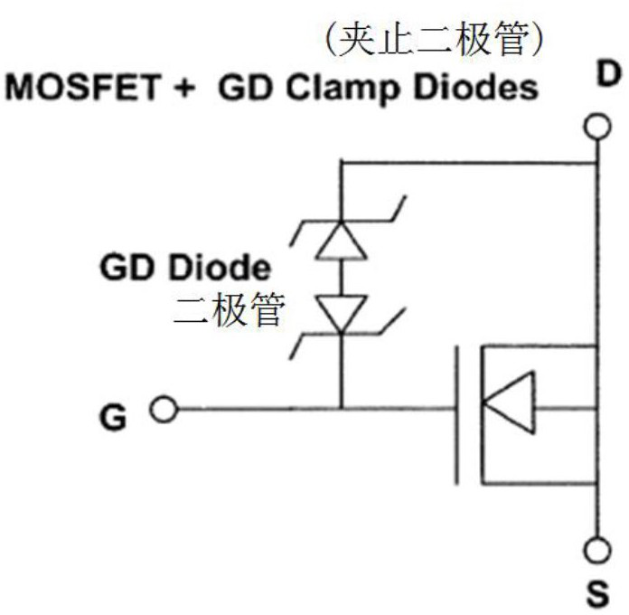
[0056] The gate-drain clamping structure of the present invention is suitable for any existing power metal oxide semi-field effect transistor, as long as the polysilicon layer 4 is continuously surrounded from the inner gate metal layer 7-2 to the other end and the outer The ring-drain metal layer 7-1 is connected, and the polysilicon layer 4 is designed so that a plurality of N-type polysilicon layers 4-2 and a plurality of P-type polysilicon layers 4-1 are continuously interleaved with each other.


PUM

PropertyMeasurementUnit
Thicknessaaaaaaaaaa
Thicknessaaaaaaaaaa
Thicknessaaaaaaaaaa

Abstract

The invention discloses a gate-drain terminal clamping structure of a planar power MOSFET device, which is characterized in that a field oxide layer is located on the upper surface of a terminal region, a polycrystalline silicon layer is located on the upper surface of the field oxide layer, a dielectric layer is located on the upper surface of the field oxide layer and wraps the polycrystalline silicon layer, and a gate metal layer and a drain metal layer are both located on the upper surface of the dielectric layer; the gate metal layer is arranged along the inner circle of the terminal area, the drain metal layer is arranged along the outer circle of the terminal area, one end of the polycrystalline silicon layer continuously surrounds the inner circle of gate metal layer to the other end circle by circle and is connected with the outer circle of drain metal layer, and the polycrystalline silicon layer comprises a plurality of N-type polycrystalline silicon layers and a plurality of P-type polycrystalline silicon layers. And the P-type polycrystalline silicon layers and the N-type polycrystalline silicon layers are continuously and mutually staggered. The polycrystalline silicon in the terminal area is connected from the gate end of the inner ring to the drain end of the periphery in a surrounding mode, boron and phosphorus are doped in a spaced mode to form multiple PN structures, the influence on reverse breakdown voltage of an assembly is little, and therefore the reliability and the voltage resistance of a product are guaranteed.

Description

technical field [0001] The invention belongs to the field of electronic components, in particular to a gate-drain clamp structure of a planar power MOSFET device. Background technique [0002] As global technology usage increases, manufacturers in all industries are pushing for higher-end performance while trying to strike a balance between their high-end performance solutions and their product reliability solutions. Technicians are faced with the challenge of balancing design complexity, reliability and cost. From the perspective of protecting the components, additional costs will be added to the components, otherwise the protection of the components cannot be achieved to achieve product reliability and safety. Therefore, if the current or voltage withstand capability of the component itself is high enough, or the component itself has a protection function, the cost can be greatly reduced. [0003] For the metal oxide semiconductor field effect transistor (Power MOSFET) o...

Claims


Application Information

Patent Timeline
IPC IPC(8): H01L29/06H01L29/78
CPCH01L29/78H01L29/0615
Inventor 李振道孙明光
Owner 南京融芯微电子有限公司