Metal organic chemical vapor deposition apparatus and deposition method

A metal-organic chemistry and vapor deposition technology, which is applied in chemical instruments and methods, post-processing devices, gaseous chemical plating, etc., can solve problems such as film difficulties, blocked film delivery pipelines, and unstable reactants.

Inactive Publication Date: 2004-08-04
HYUNDAI ELECTRONICS IND CO LTD
View PDF0 Cites 0 Cited by
  • Summary
  • Abstract
  • Description
  • Claims
  • Application Information

AI Technical Summary

Problems solved by technology

Also, the reactant cannot be stably supplied to the reactor because the decomposed reactant clogs the film transfer line between the evaporator and the reactor
Therefore, it is very difficult to form thin films with reliable and excellent electrical properties

Method used


Image

  • Metal organic chemical vapor deposition apparatus and deposition method
  • Metal organic chemical vapor deposition apparatus and deposition method
  • Metal organic chemical vapor deposition apparatus and deposition method

Examples


Embodiment Construction

[0018] The preferred embodiments of the present invention can be better understood with reference to the accompanying drawings.

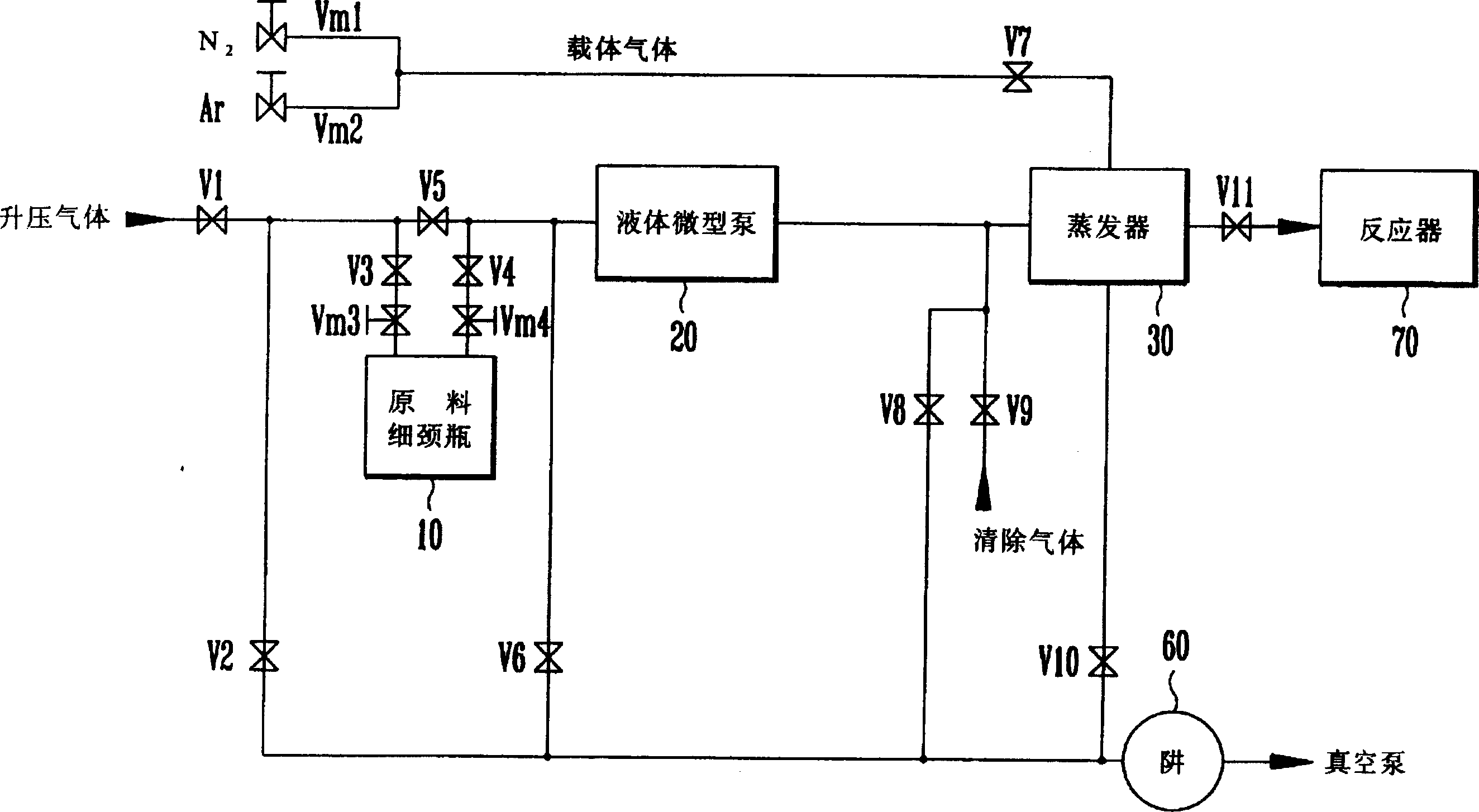
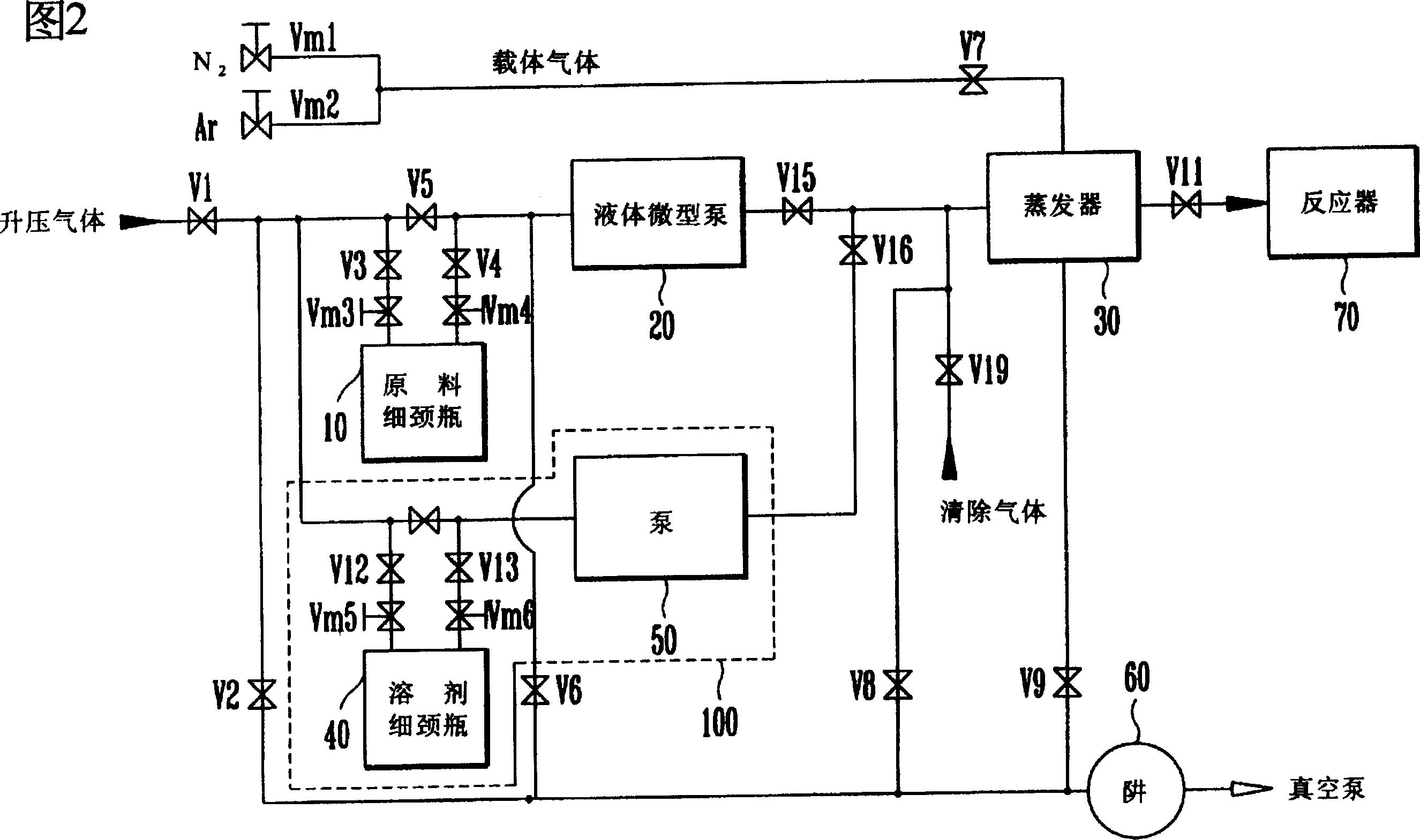
[0019] Referring to Fig. 2, it shows the MOCVD apparatus of the present invention. As shown in the figure, the MOCVD device of the present invention is the same as the conventional device in that it includes a raw material ampoule 10, a liquid micropump 20, and an evaporator for evaporating the liquid reactant that are dissolved in a solvent. 30. A reactor 70 for depositing reactants on a semiconductor substrate, a trap 60 for sealing harmful gases by cooling, and a vacuum pump, the difference is that the evaporator 30 is further equipped with a solvent supply device 100, which includes a solvent flask 40 and pump 50.

[0020] The process of forming a high dielectric film will be described below based on this diagram.

[0021] The reactant can use Ba(DPM) 2 , Sr(DPM) 2 and Ti(OC 3 h 7 ) 4 or Ti[OCH(CH 3 ) 2 ] 2 (DPM) 2 (DPM is dipivaloylm...


PUM


Abstract

A metal organic chemical vapor deposition apparatus comprising a source ampule, a liquid micro-pump, a vaporizer equipped with a solvent supply means, and a reactor. A reactant dissolved in a solvent in the source ampule is transferred to the vaporizer by the liquid micro-pump. A sufficient amount of the solvent is additionally fed to the vaporizer by the solvent supply means, concurrently with the transfer, and vaporized along with the reactants. After being vaporized in the vaporizer, the reactant is injected to the reactor by carrier gas and deposited on a semiconductor substrate to form a high dielectric thin film. By virtue of the additional supplied solvent, the recondensation of the reactant in the vaporizer, can be prevented in the vaporizer and in the transfer line between the vaporizer and the reactor. In addition, the residues of the reactant can be washed off by providing the solvent through the supply means to the vaporizer.

Description

technical field [0001] The present invention relates to metal organic chemical vapor deposition (hereinafter referred to as "MOCVD") apparatus and deposition method. More particularly, the present invention relates to an MOCVD apparatus for depositing a high dielectric thin film on a semiconductor substrate, and a deposition method using the apparatus. Background technique [0002] The memory capacity of the next-generation DRAM is at least 1Giga, and the traditional thin film cannot provide enough capacity. As the size of semiconductors is getting smaller and smaller, three-dimensional capacitor structures like fins and cylinders are becoming more and more difficult to manufacture, because the size reduction must reduce the cell area at the same time. [0003] In addition, the reduction in film thickness increases the leakage current in the power / drain region (the impure region on the semiconductor device) and causes soft errors, which are data stored in the capacitor chan...

Claims


Application Information

Patent Timeline
Patent Type & Authority Patents(China)
IPC IPC(8): C30B35/00C23C16/40C23C16/44C23C16/448C23C16/455H01L21/203H01L21/31
CPCC23C16/4481C23C16/409C23C16/455
Inventor 刘尤植白熔求朴泳震金钟哲
Owner HYUNDAI ELECTRONICS IND CO LTD
Why Eureka
Try Eureka