Unlock instant, AI-driven research and patent intelligence for your innovation.

Nitride read-only memory structure and mfg. method thereof

A technology of read-only memory and manufacturing method, applied in semiconductor/solid-state device manufacturing, electric solid-state device, semiconductor device and other directions, can solve the problems of source/drain lateral diffusion, the limit limitation of component miniaturization, etc., to reduce heat Budget, ensure stability, reduce the effect of lateral spread

Inactive Publication Date: 2004-10-27
MACRONIX INT CO LTD
View PDF1 Cites 0 Cited by
  • Summary
  • Abstract
  • Description
  • Claims
  • Application Information

AI Technical Summary

Problems solved by technology

However, this manufacturing method causes severe lateral diffusion of the source / drain, which limits the miniaturization limit of components.

Method used


Image

  • Nitride read-only memory structure and mfg. method thereof
  • Nitride read-only memory structure and mfg. method thereof
  • Nitride read-only memory structure and mfg. method thereof

Examples


Embodiment Construction

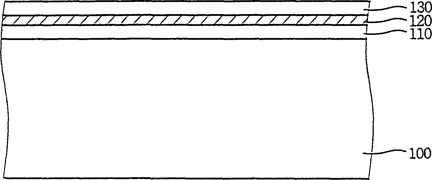
[0023] Please refer to Figures 1A-1E , which shows a cross-sectional view of the manufacturing process of a nitride read-only memory according to a preferred embodiment of the present invention.

[0024] exist Figure 1A In this method, a bottom oxide layer 110 , a silicon nitride layer 120 and a top oxide layer 130 are sequentially formed on the substrate 100 . The bottom oxide layer 110 is preferably formed by thermal oxidation, and the silicon nitride layer 120 is preferably formed by low pressure chemical vapor deposition. Then thermal oxidation is performed to oxidize the surface layer of the silicon nitride layer 120 into a top oxide layer 130, so the initial deposition thickness of the silicon nitride layer 120 must be thicker to compensate for the part lost due to oxidation later. The thicknesses of the silicon nitride layer 120 after the formation of the bottom oxide layer 110 and the top oxide layer 130 are preferably about 50-90 angstroms and 40-70 angstroms, resp...


PUM


Abstract

A nitride ROM with high integrated level is composed of composite grid dielectric layer on substrate, which is composed of bottom oxide layer, silicon nitride layer and top oxide layer, the silicon oxide layer on the surface of said grid dielectric layer, bit line oxide layer in the substrate at both sides of said composite grid dielectric layer, the source / drain in the substrate under bit line oxide layer, and grid cross the grid dielectric layer and on the bit line oxide layer.

Description

technical field [0001] The present invention relates to a structure of a semiconductor component and a manufacturing method thereof, in particular to a structure of a nitride read only memory (NROM) and a manufacturing method thereof. Background technique [0002] With the improvement of integrated circuit technology and the popularization of information product applications, semiconductor components are becoming increasingly important. Among them, memory plays a key role in the application of information products, especially flash memory with superior data storage characteristics has gradually become the mainstream of the non-volatile memory market. However, due to the increasingly shrinking line width of semiconductor components, power-saving design considerations, data signal level degradation, and external noise interference, it is difficult to accurately control the signal level of flash memory when writing or erasing data signals. In other words, electrons cannot be e...

Claims


Application Information

Patent Timeline
Patent Type & Authority Patents(China)
IPC IPC(8): H10B20/00
Inventor 刘振钦
Owner MACRONIX INT CO LTD