Unlock instant, AI-driven research and patent intelligence for your innovation.

Process for preparing flash memory

A manufacturing method and flash memory technology, applied in the field of flash memory manufacturing, can solve the problems of short channel effect, inability to solve short channel effect at the same time, breakdown leakage current and load effect, inability to effectively reduce, etc., so as to improve the breakdown leakage current , improve the short channel effect, improve the effect of the load effect

Inactive Publication Date: 2005-07-06
MACRONIX INT CO LTD
View PDF0 Cites 0 Cited by
  • Summary
  • Abstract
  • Description
  • Claims
  • Application Information

AI Technical Summary

Problems solved by technology

When we use the method of channel hot electron injection to program components, we must supply a large bias voltage to the source / drain, but the substantial bias voltage becomes smaller due to the voltage drop, resulting in a serious loading effect (loading effect)
[0006] To sum up the above, in the case of shrinking component specifications, if a shallow drain junction is used to solve the short channel effect and breakdown leakage current, it will lead to the generation of source / drain loading effect
Conversely, deepening the drain junction in order to solve the loading effect will lead to short channel effect and breakdown leakage current
It can be seen that the known flash memory manufacturing methods cannot solve the problems of short channel effect, breakdown leakage current and load effect at the same time, so that the manufacture of components cannot be effectively reduced.

Method used


Image

  • Process for preparing flash memory
  • Process for preparing flash memory
  • Process for preparing flash memory

Examples


Embodiment Construction

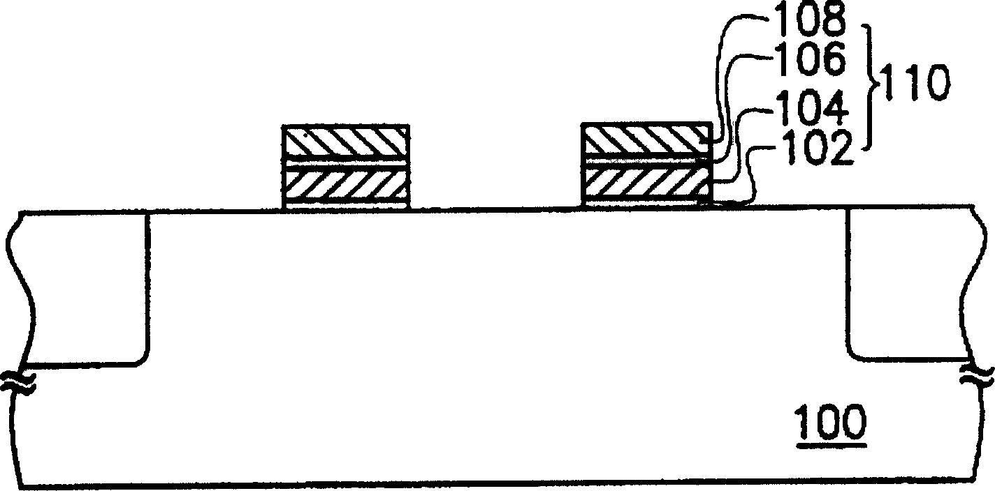
[0030] Figure 1A to Figure 1D It is a schematic cross-sectional view of a manufacturing process of a flash memory in a preferred embodiment of the present invention.

[0031] First, please refer to Figure 1A , provide a substrate 100, and form a stacked gate 110 composed of a tunnel oxide layer 102, a floating gate 104, a dielectric layer 106, and a control gate 108 on the substrate 100. The method of forming the stacked gate 110 may be on the substrate 100 sequentially forming a thermal oxide layer (not shown in the figure), a first conductor layer (not shown in the figure), an oxide layer (not shown in the figure) and a second conductor layer (not shown in the figure); then, Define a thermal oxide layer, a first conductor layer, an oxide layer, and a second conductor layer, and form a stack gate 110 composed of a tunnel oxide layer 102, a floating gate 104, a dielectric layer 106, and a control gate 108 on the substrate 100 , and expose the substrate 100 on both sides of ...


PUM


Abstract

A method for manufacturing flash memory. A shallow junction doping step is performed on a substrate with stacked gates as a mask, and shallow junction doped regions are formed in the substrates on both sides of the stacked gates. Next, a mask layer is formed on the substrate, wherein the mask layer covers the surface and sidewalls of the stacked gate, and exposes part of the shallow junction doped region. Then, the substrate is subjected to a deep junction doping step using the mask layer as a mask, and deep junction doping regions are formed in the substrate on both sides of the mask layer. Finally, a thermal process is performed after removing the mask layer to form source / drain regions with shallow drain junctions and deep drain junctions.

Description

technical field [0001] The invention relates to a manufacturing method of a memory, and in particular to a manufacturing method of a flash memory (flash memory). Background technique [0002] Flash memory is a kind of read-only memory (non-volatile memory), which has the advantages of being writable, erasable, and can still save data after power failure. It is a memory component widely used in personal computers and electronic devices. . [0003] The known method of forming a transistor memory cell is to perform an ion doping step on the substrate with the stacked gate as a mask after completing the stacked gate composed of the tunnel oxide layer, floating gate, dielectric layer, control gate, etc., and then After tempering at high temperature and for a long time, a source / drain region with a deep junction is formed. The source / drain region can generate hot electrons in the channel by channel hot electron injection (channel hot electron injection) method after applying an ...

Claims


Application Information

Patent Timeline
Patent Type & Authority Patents(China)
IPC IPC(8): H10B20/00
Inventor 范左鸿蔡文哲卢道政
Owner MACRONIX INT CO LTD