

Process for making double inlay structure for preventing positioning error
A technology of double damascene structure and manufacturing process, which is applied in the photolithographic process of pattern surface, semiconductor/solid-state device manufacturing, and photosensitive materials used in optomechanical equipment, etc., which can solve positioning errors and uneven photoresist thickness Equilibrium problem to achieve the effect of avoiding positioning errors
- Summary
- Abstract
- Description
- Claims
- Application Information
AI Technical Summary
Problems solved by technology
Method used
Image

Examples
Embodiment Construction
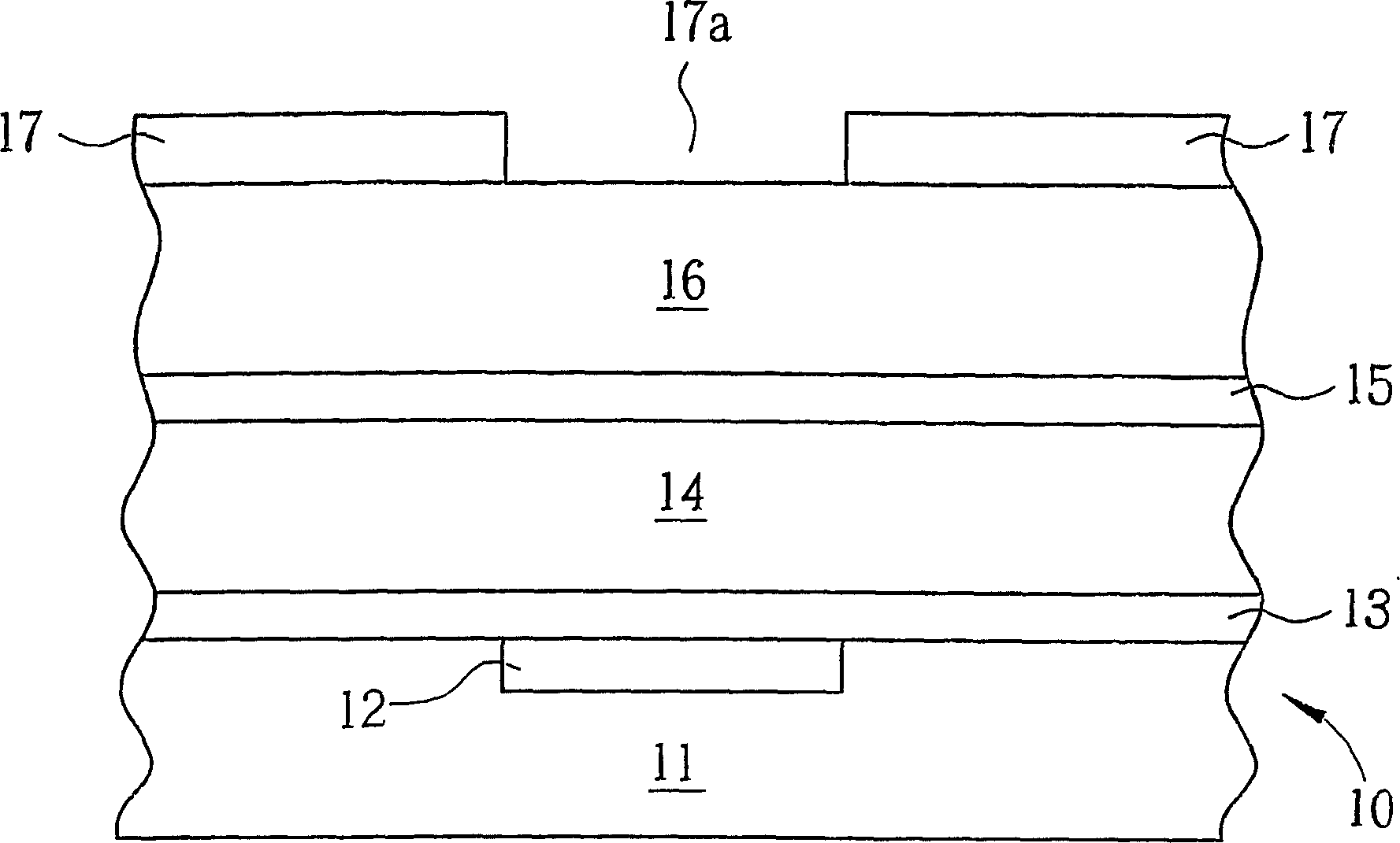
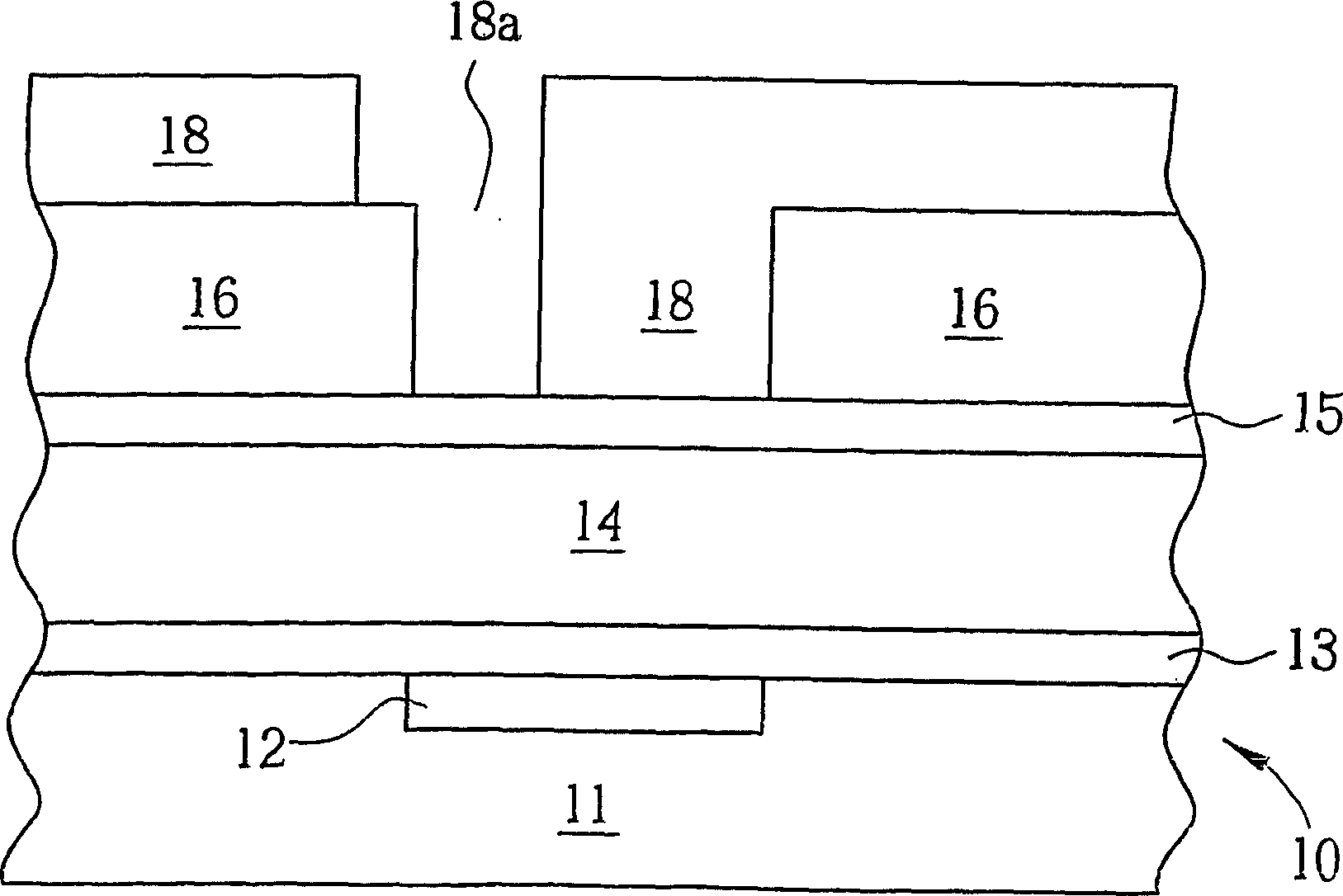
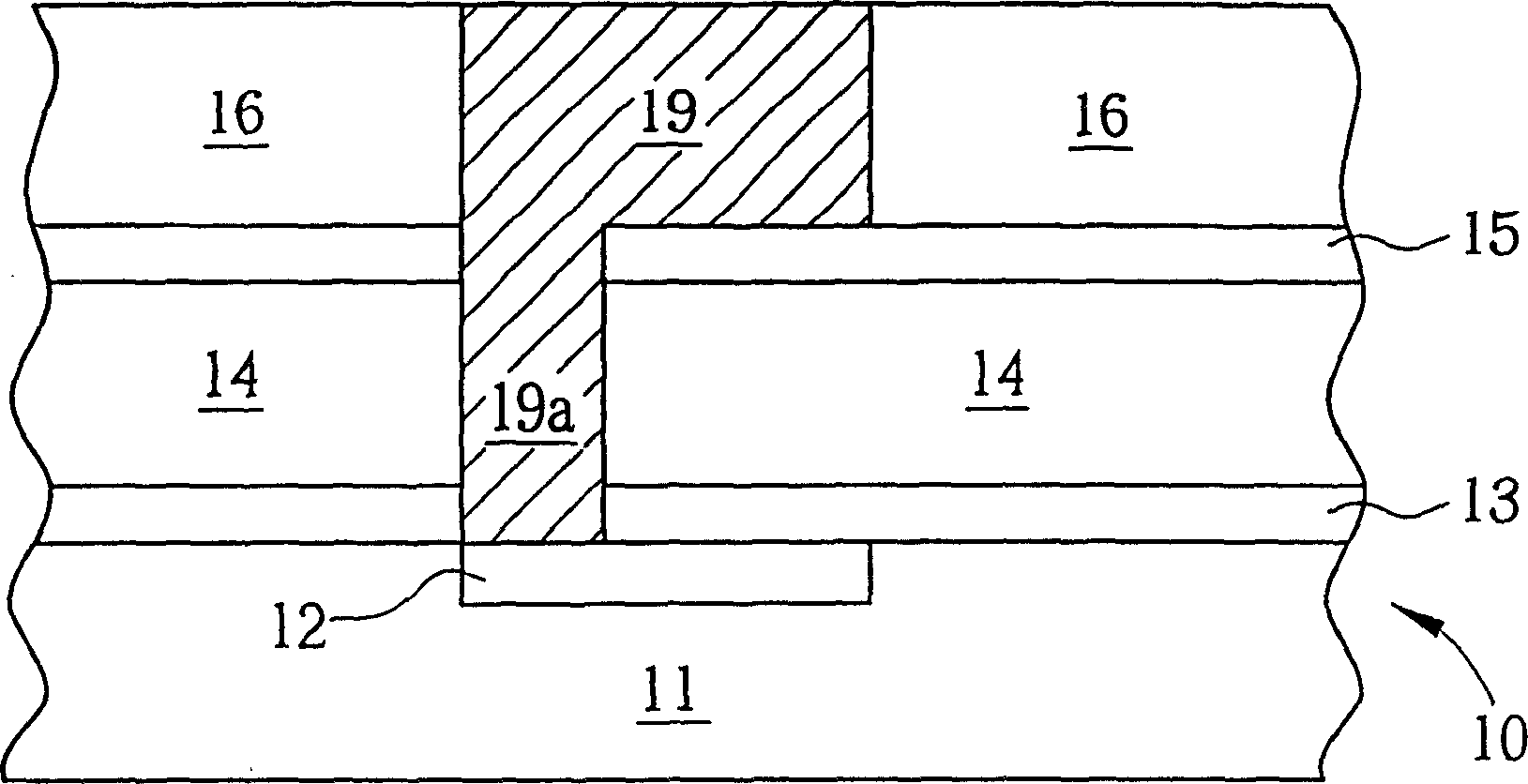
[0030] see Figure 4 to Figure 9 , Figure 4 to Figure 9 It is a schematic diagram of the method for fabricating a dual damascene structure on a semiconductor chip according to the present invention. Such as Figure 4 As shown, a semiconductor chip 20 includes a conductive layer substrate 22 , a passivation layer 24 formed on the conductive layer substrate 22 , and a dielectric layer 26 formed on the passivation layer 24 . First, a photoresist layer 28 is coated on the surface of the dielectric layer 26, and an opening is formed in the photoresist layer 28 through a photolithography process including exposure, development and cleaning. 28a to define the trench positions in the dual damascene structure. In a preferred embodiment of the present invention, the conductive layer base 22 is made of copper metal, and the dielectric layer 26 can be made of silicon oxide, fluorosilicate glass (FSG) or a dielectric material with a dielectric constant lower than 3 (such as SiLK TM ),...
PUM
| Property | Measurement | Unit |
|---|---|---|
| power | aaaaa | aaaaa |
Abstract
Description
Claims
Application Information